- Current Research > Terahertz Emission from Semiconductors: Carrier Dynamics Modelling and Experiment
- We have developed a three dimensional carrier
dynamics simulation to model ultrafast processes in, and terahertz
emission from photo-excited semiconductors. This page contains a description of the simulation and some examples of its application to understanding a number of important issues in terahertz science and technology. For enquires please contact Michael Johnston.
- Description of the carrier dynamics model
-
 |
The simulation is a semi-classical Monte Carlo simulation capable of
modelling hot carrier dynamics in most inorganic semiconductors. It
models both intrinsic and extrinsic electron and hole distributions,
considering electron populations in Gamma, X and L valleys. Classical
trajectories are calculated for pseudo-particles (typically ~1
million) over short time intervals (~1fs). At the end of each time
step scattering rates and angles are calculated quantum mechanically
for each pseudo particle in the distribution and a random number
generator is used to determine the particle scatters or not. THz
emission is calculated based on the net acceleration of charge
carriers in the distributions. Each simulation produces huge amounts
of data, including 3D carriers distributions and scattering rates at
each specified time step.
See:
- Phys. Rev. B, 65 (2002), p. 165301.
[ bib |
http |
.ps.gz |
.pdf ]
A detailed description of the original simulation
- Phys. Rev. B, 71 (2005), p. 195301.
[ bib |
http |
.ps.gz |
.pdf ]
Extension of the simulation which allows photoconductive switches and antennae to be modelled
|
- THz generation from semiconductor surfaces - the relative importance of surface field and photo-Dember mechanisms
-
 |
When a sub-picosecond laser pulse if is absorbed at the surface of a semiconductor it is found that a single cycle terahertz transient is emitted. There are two main mechanisms by which charge may be accelerated leading to terahertz emission - the surface field effect (a result of Fermi level pinning and band banding) and the photo-Dember effect (a result of a difference in the mobility of different charge carries types and an asymmetry cause by the semiconductor's surface). The surface of InAs is a very efficient generator of THz radiation. Why is this so? Understanding the mechanism of THz generation from InAs and GaAs allows us to answer this question.
Our modelling shows that InAs is primarily a photo-Dember emitter
while GaAs is primarily a surface field emitter. In addition the
simulations reproduce the large THz electric-field amplitudes and
hence powers observed experimentally in InAs when compared with GaAs.
See: - Phys. Rev. B, 65 (2002), p. 165301. [ bib | http | .ps.gz
| .pdf
]
Section III presents a explanation of the THz generation mechanisms in InAs and GaAs as well as the simulation results for these materials
|
- The mechanism of magnetic field enhanced THz generation
-
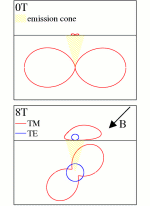 |
A large magnetic field can increase the THz power radiated from a photo-excited surfaces of semiconductors such as InAs and GaAs by an order of magnitude. Magnetic field enhancement effects are also seen in other surface field/photo-Dember THz emitters. There has been much discussion over the mechanism of this effect.
After performing carrier dynamics Monte Carlo simulations we concluded
that the main effect of the Lorentz force is to reorientate the THz
dipole with respect to the surface of the semiconductor, with little
change to the dipole strength. The observed increase in emitted THz
power is due to the increased transmission of THz radiation through
the surface of the semiconductor in the new dipole orientation.
See:
- J. Appl. Phys., 91 (2002), pp. 2104-2106.
[ bib |
http |
.ps.gz |
.pdf ]
Experimental and theoretical modelling of THz emission from GaAs, showing a very good agreement.
- Appl. Phys. Lett., 76 (2000), pp. 2038-2040.
[ bib |
http |
.ps.gz
Experimental paper showing magnetic field enhancement of THz emission from InAs
- Phys. Rev. B, 65 (2002), p. 165301.
[ bib |
http |
.ps.gz |
.pdf ]
Theoretical modelling of magnetic field enhanced THz emission from GaAs and InAs, along with detailed description of the model
|
- THz generation from photoconductive switches / antennae, including anode enhancement effects
-
 |
Photoconductive switches are the most popular THz single cycle
emitters due to the high field they produce. Studying the influence
of experimental parameters such as the bias voltage, excitation
pulse duration and location across the gap on the emitted transient
is highly relevant in order to improve the characteristics of such
emitters.
See:
- Phys. Rev. B, 71 (2005), p. 195301.
[ bib |
http |
.pdf ]
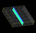
Simulation of carrier dynamics in a biased photoconductive switch.
|
- Influence of surface-passivation on ultrafast conductivity and terahertz radiation generation in GaAs
-
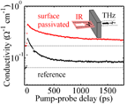 Ultrafast conductivity of photoexcited electrons in GaAs doubles after surface passivation.
|
The carrier dynamics of photoexcited electrons in the vicinity of the surface of (NH4)2S-passivated GaAs were studied via terahertz (THz) emission spectroscopy and optical-pump THz-probe spectroscopy. THz emission spectroscopy measurements, coupled with Monte Carlo simulations of THz emission, revealed that the surface electric field of GaAs reverses after passivation. The conductivity of photoexcited electrons was determined via optical-pump THz-probe spectroscopy, and was found to double after passivation. These experiments demonstrate that passivation significantly reduces the surface state density and surface recombination velocity of GaAs. Finally, we have demonstrated that passivation leads to an enhancement in the power radiated by photoconductive switch THz emitters, thereby showing the important influence of surface chemistry on the performance of ultrafast THz photonic devices.
See:
|
- Optimisation of ion damaged materials for broad-bandwidth THz emitters
-
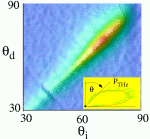
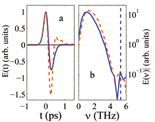 Relative power at high frequencies is larger for an implanted (red lines) than an unimplanted (blue) InP:Fe photoconductive switch. |
Damaging a semiconductor crystal by bombarding it with energetic ions can create defects that trap and scatter photoexcited carriers on ultra-short timescales. This can shorten the duration of a terahertz pulse, by reducing the time it takes for photoexcited electrons to decelerate, and increase the bandwidth of THz emission.
We have studied the carrier dynamics of the ion-implanted semiconductors GaAs:As,
InP:Fe, InP:O and InGaAs:Fe via a combination of:
- optical-pump, THz-probe experiments, to measure the lifetime and photoexcited conductivity
- THz emission measurements from semiconductor surfaces and photoconductive switches
- simulations of the influence of carrier-defect scattering and carrier trapping on THz emission
See:
- Phys. Rev. B, 70 (2004), p. 235330. [ bib | http | .ps.gz | .pdf ]
An experimentally observed increase in frequency of peak terahertz emission power
is attributed to ultrafast carrier trapping by comparison with simulation work.
- Proc. SPIE, 6118 (2006), p. 61180K.
[ http |
.pdf ]
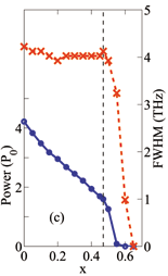
InGaAs:Fe surface emitters and InP:Fe photoconductive switches emit more THz power at
high frequencies with increasing ion dose (shorter carrier lifetime).
|
- Suitable materials for terahertz emitters and detectors excited with 1.55μm lasers
-
 |
The use of a low-bandgap semiconductor such as In1-xGaxAs (with x<0.47)
would enable cheaper, turnkey THz spectroscopy setups based on erbium fibre lasers, which can produce
pulses as short as 65fs at a wavelength of 1.55μm. Combining a compact system of this type with
communications wavelength optical fibres would enable THz pulses to be generated and detected
in small, extreme, or otherwise inaccessible environments (e.g. in an endoscope, or in the cavity of
a pulsed magnet).
We have used our carrier dynamics model to simulate THz emission from InGaAs excited by pulses from
tunable 1.55μm erbium fibre lasers, and find that emitted field strengths should be comparable to those obtained from GaAs excited at 800nm. We observe an increase in the emitted power as the alloy approaches InAs (see figure on left).
See:
- Sol. Stat. Comm, 136 (2005), p. 136595.
[ bib |
http |
.pdf ]
Comparison of THz emission from InGaAs, InP, using our carrier dynamics simulation.
- Proc. SPIE, 6118 (2006), p. 61180K.
[ bib |
http |
.pdf ]
InGaAs:Fe surface emitters excited at 800nm emit more THz power at
high frequencies with increasing ion dose (shorter carrier lifetime).
|
|
|
|