- Journal Publications - Icon View
- Control over the microstructure of vapour-deposited cspbbr3 enhances amplified spontaneous emission
-
 | Q Yuan, W Li, JE Lee, F Wagner, VJ Lim, LM Herz, J Etheridge, MB Johnston
Adv. Optical Mater., 13:e02160 (Sep 2025)
[
pdf ][ SI ][ ref ]
Inorganic cesium-based metal halide perovskite (MHP) semiconductors have great potential as active layers in optoelectronic devices, such as perovskite light-emitting diodes (PeLEDs) and perovskite lasers. However, precise control of crystal type, quality, and thickness is required to create high-performance and reproducible devices. Vapor-phase vacuum deposition enables fabrication of MHP thin films and devices with excellent uniformity and control over layer thickness, although a full understanding of crystal growth mechanisms and products has proved elusive.
Here, conditions of vapor co-deposition of CsBr and PbBr$_2$ are related with the optical performance and atomic microstructure of resulting CsPbBr$_3$ thin films. It is found that the structure is predominantly photoactive $\gamma$-CsPbBr$_3$ over a wide range of conditions, but the presence of impurity phases and Ruddlesden--Popper (RP) planar defects both degrade optical performance as quantified through measured amplified spontaneous emission (ASE) thresholds. Furthermore, the atomic structure of the dominant impurity phases is resolved: CsPb$_2$Br$_5$ and Cs$_4$PbBr$_6$.
It is revealed that a small nominal excess of CsBr-precursor flux during co-evaporation can significantly enhance the nucleation of thin films, resulting in well-defined grains greater than 500~nm in size and the relative suppression of RP planar defects. Such films exhibit intensified photoluminescence (PL) emission and a reduced ASE threshold of 30.9~$\mu$J\,cm$^{-2}$.
|
- The influence of subwavelength geometry on extracting the electrical properties of semiconductors by terahertz spectroscopy
-
 | FM Wagner, T Haggren, JC Bürger, TJ Keat, K Peng, C Uswachoke, DA Damry, H Kraus, HJ Joyce, HH Tan, C Jagadish, T Siday, MB Johnston
APL Photonics, 10:076123 (Jul 2025)
[
pdf ][ SI ][ ref ]
Terahertz (THz) spectroscopy is a non-contact technique well-suited for probing the ultrafast electrical conductivity of semiconductor nanostructures, where conventional methods are often impractical. However, geometric resonances in these nanostructures can distort the measured THz response, complicating the extraction of the intrinsic material properties. Here, we use THz spectroscopy to study GaAs nanowires of varying lengths and observe that the resonant frequency increases as the nanowire length decreases. Further measurements on a model system of well-defined GaAs microsquares (ranging in size from 500 x 500 to 7 x 7 mu m(2)) confirmed the relationship between structure size and resonant frequency. We verify that a plasmon-based model successfully separates the geometric response from the intrinsic charge-carrier response. Thus, the model allows for the accurate evaluation of critical material properties in nanostructured semiconductors, such as electron mobility. Fluence-dependent measurements and finite-difference time-domain simulations confirm the plasmonic nature of the resonances. (c) 2025 Author(s). All article content, except where otherwise noted, is licensed under a Creative Commons Attribution (CC BY) license
|
- Inter-layer diffusion of excitations in 2D perovskites revealed by photoluminescence reabsorption
-
 | JX Du, M Righetto, M Kober-czerny, SY Yan, KA Elmestekawy, HJ Snaith, MB Johnston, LM Herz
Adv. Funct. Mater., 35:2421817 (Jun 2025)
[
pdf ][ SI ][ ref ]
2D lead halide perovskites (2DPs) offer chemical compatibility with 3D perovskites and enhanced stability, which are attractive for applications in photovoltaic and light-emitting devices. However, such lowered structural dimensionality causes increased excitonic effects and highly anisotropic charge-carrier transport. Determining the diffusivity of excitations, in particular for out-of-plane or inter-layer transport, is therefore crucial, yet challenging to achieve. Here, an effective method is demonstrated for monitoring inter-layer diffusion of photoexcitations in (PEA)2PbI4 thin films by tracking time-dependent changes in photoluminescence spectra induced by photon reabsorption effects. Selective photoexcitation from either substrate- or air-side of the films reveals differences in diffusion dynamics encountered through the film profile. Time-dependent diffusion coefficients are extracted from spectral dynamics through a 1D diffusion model coupled with an interference correction for refractive index variations arising from the strong excitonic resonance of 2DPs. Such analysis, together with structural probes, shows that minute misalignment of 2DPs planes occurs at distances far from the substrate, where efficient in-plane transport consequently overshadows the less efficient out-of-plane transport in the direction perpendicular to the substrate. Through detailed analysis, a low out-of-plane excitation diffusion coefficient of (0.26 +/- 0.03) x10-4 cm2 s-1 is determined, consistent with a diffusion anisotropy of approximate to 4 orders of magnitude.
|
- Aerosol-assisted crystallization lowers intrinsic quantum confinement and improves optoelectronic performance in fapbi3 films
-
 | G Kaur, M Hameed, JE Lee, KA Elmestekawy, MB Johnston, J Briscoe, LM Herz
J. Phys. Chem. Lett., 16:2212-2222 (Feb 2025)
[
pdf ][ SI ][ ref ]
FAPbI3 has emerged as a promising semiconductor for photovoltaic applications offering a suitable bandgap for single-junction cells and high chemical stability. However, device efficiency is negatively affected by intrinsic quantum confinement (QC) effects that manifest as additional peaks in the absorption spectra. Here, we show that aerosol-assisted crystallization is an effective method to improve crystallinity and suppresses regions exhibiting QC in FAPbI3. We demonstrate that films with minimized QC effects exhibit markedly enhanced optoelectronic properties, such as higher charge-carrier mobilities and recombination lifetimes. Films crystallized under an aerosol solvent flow of either a mixture of N,N-dimethylformamide and dimethyl sulfoxide or methylammonium thiocyanate vapor displayed reduced charge-carrier recombination losses and improved diffusion lengths compared to those of thermally annealed control films. Our study indicates clear correlations between suppression of QC features in absorption spectra with optimization of crystallinity and mitigation of internal strain, highlighting pathways toward high-performance solar cells.
|
- Resonance-amplified terahertz near-field spectroscopy of a single nanowire
-
 | S Norman, G Chu, K Peng, J Seddon, LL Hale, HH Tan, C Jagadish, R Mouthaan, J Alexander-webber, HJ Joyce, MB Johnston, O Mitrofanov, T Siday
Nano Lett., 24:15716--15723 (Nov 2024)
[
pdf ][ SI ][ ref ]
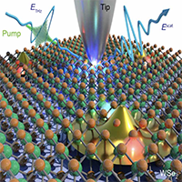
Nanoscale material systems are central to next-generation optoelectronic and quantum technologies, yet their development remains hindered by limited characterization tools, particularly at terahertz (THz) frequencies. Far-field THz spectroscopy techniques lack the sensitivity for investigating individual nanoscale systems, whereas in near-field THz nanoscopy, surface states, disorder, and sample-tip interactions often mask the response of the entire nanoscale system. Here, we present a THz resonance-amplified near-field spectroscopy technique that can detect subtle conductivity changes in isolated nanoscale systems-such as a single InAs nanowire-under ultrafast photoexcitation. By exploiting the spatial localization and resonant field enhancement in the gap of a bowtie antenna, our approach enables precise measurements of the nanostructures through shifts in the antenna resonant frequency, offering a direct means of extracting the system response, and unlocking investigations of ultrafast charge-carrier dynamics in isolated nanoscale and microscale systems.
|
- In situ nanoscopy of single-grain nanomorphology and ultrafast carrier dynamics in metal halide perovskites
-
 | M Zizlsperger, S Nerreter, Q Yuan, KB Lohmann, F Sandner, F Schiegl, C Meineke, YA Gerasimenko, LM Herz, T Siday, MA Huber, MB Johnston, R Huber
Nat. Photon., 18:975–-981 (Sep 2024)
[
pdf ][ SI ][ ref ]
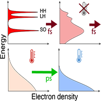
Designing next-generation light-harvesting devices requires a detailed understanding of the transport of photoexcited charge carriers. The record-breaking efficiencies of metal halide perovskite solar cells have been linked to effective charge-carrier diffusion, yet the exact nature of charge-carrier out-of-plane transport remains notoriously difficult to explain. The characteristic spatial inhomogeneity of perovskite films with nanograins and crystallographic disorder calls for the simultaneous and hitherto elusive in situ resolution of the chemical composition, the structural phase and the ultrafast dynamics of the local out-of-plane transport. Here we simultaneously probe the intrinsic out-of-plane charge-carrier diffusion and the nanoscale morphology by pushing depth-sensitive terahertz near-field nanospectroscopy to extreme subcycle timescales. In films of the organic-inorganic metal halide perovskite FA0.83Cs0.17Pb(I1-xClx)3 (where FA is formamidinium), domains of the cubic alpha-phase are clearly distinguished from the trigonal delta-phase and PbI2 nano-islands. By analysing deep-subcycle time shifts of the scattered terahertz waveform after photoexcitation, we access the vertical charge-carrier dynamics within single grains. At all of the measured locations, despite topographic irregularities, diffusion is surprisingly homogeneous on the 100 nm scale, although it varies between mesoscopic regions. Linking in situ carrier transport with nanoscale morphology and chemical composition could introduce a paradigm shift for the analysis and optimization of next-generation optoelectronics that are based on nanocrystalline materials. Transient visible-pump terahertz-probe near-field microscopy enables the simultaneous retrieval of the local chemical composition, crystallographic structure, topography and out-of-plane charge-carrier diffusion in perovskite films.
Citations: 35 (Scopus) 28 (Web of Science) |
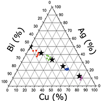
- The role of chemical composition in determining the charge-carrier dynamics in $(AgI)_x(BiI_3)_y$ rudorffites
-
 | S Lal, M Righetto, BWJ Putland, HC Sansom, SG Motti, H Jin, MB Johnston, HJ Snaith, LM Herz
Adv. Funct. Mater., 34:2315942 (Aug 2024)
[
pdf ][ SI ][ ref ]
Silver-bismuth-based perovskite-inspired materials (PIMs) are increasingly being explored as non-toxic materials in photovoltaic applications. However, many of these materials exhibit an ultrafast localization of photogenerated charge carriers that is detrimental for charge-carrier extraction. In this work, such localization processes are explored for thermally evaporated thin films of compositions lying along the (AgI)x(BiI3)y series, namely BiI3, AgBi2I7, AgBiI4, Ag2BiI5, Ag3BiI6, and AgI, to investigate the impact of changing Ag+/Bi3+ content. A persistent presence of ultrafast charge-carrier localization in all mixed compositions and BiI3, together with unusually broad photoluminescence spectra, reveal that eliminating silver will not suppress the emergence of a localized state. A weak change in electronic bandgap and charge-carrier mobility reveals the resilience of the electronic band structure upon modifications in the Ag+/Bi3+ composition of the mixed-metal rudorffites. Instead, chemical composition impacts the charge-carrier dynamics indirectly via structural alterations: Ag-deficient compositions demonstrate stronger charge-carrier localization most likely because a higher density of vacant sites in the cationic sublattice imparts enhanced lattice softness. Unraveling such delicate interplay between chemical composition, crystal structure, and charge-carrier dynamics in (AgI)x(BiI3)y rudorffites provides crucial insights for developing a material-by-design approach in the quest for highly efficient Bi-based PIMs. The optoelectronic properties of thermally-evaporated (AgI)x(BiI3)y thin films reveal a band structure resilient to changes in chemical composition. Ultrafast, picosecond charge-carrier localization is observed for all Bi-containing compositions. The increased incorporation of structural vacancies with reducing silver content leads to stronger localization, yielding lower long-term charge-carrier mobility. Corresponding trends in extremely broad photoluminescence further validate charge localization across the series. image
Citations: 13 (Scopus) 13 (Web of Science) |
- Contrasting ultra-low frequency raman and infrared modes in emerging metal halides for photovoltaics
-
 | VJY Lim, M Righetto, SY Yan, JB Patel, T Siday, B Putland, KM McAll, MT Sirtl, Y Kominko, JL Peng, QQ Lin, T Bein, M Kovalenko, HJ Snaith, MB Johnston, LM Herz
ACS Energy Lett., 9:4127-4135 (Jul 2024)
[
pdf ][ SI ][ ref ]
Lattice dynamics are critical to photovoltaic material performance, governing dynamic disorder, hot-carrier cooling, charge-carrier recombination, and transport. Soft metal-halide perovskites exhibit particularly intriguing dynamics, with Raman spectra exhibiting an unusually broad low-frequency response whose origin is still much debated. Here, we utilize ultra-low frequency Raman and infrared terahertz time-domain spectroscopies to provide a systematic examination of the vibrational response for a wide range of metal-halide semiconductors: FAPbI(3), MAPbI(x)Br(3-x), CsPbBr3, PbI2, Cs2AgBiBr6, Cu2AgBiI6, and AgI. We rule out extrinsic defects, octahedral tilting, cation lone pairs, and \"liquid-like\" Boson peaks as causes of the debated central Raman peak. Instead, we propose that the central Raman response results from an interplay of the significant broadening of Raman-active, low-energy phonon modes that are strongly amplified by a population component from Bose-Einstein statistics toward low frequency. These findings elucidate the complexities of light interactions with low-energy lattice vibrations in soft metal-halide semiconductors emerging for photovoltaic applications.
|
- Unraveling loss mechanisms arising from energy-level misalignment between metal halide perovskites and hole transport layers
-
 | JE Lee, SG Motti, RDJ Oliver, S Yan, HJ Snaith, MB Johnston, LM Herz
Adv. Funct. Mater., 34:2401052 (Jul 2024)
[
pdf ][ SI ][ ref ]
Metal halide perovskites are promising light absorbers for multijunction photovoltaic applications because of their remarkable bandgap tunability, achieved through compositional mixing on the halide site. However, poor energy-level alignment at the interface between wide-bandgap mixed-halide perovskites and charge-extraction layers still causes significant losses in solar-cell performance. Here, the origin of such losses is investigated, focusing on the energy-level misalignment between the valence band maximum and the highest occupied molecular orbital (HOMO) for a commonly employed combination, FA0.83Cs0.17Pb(I1-xBrx)3 with bromide content x ranging from 0 to 1, and poly[bis(4-phenyl)(2,4,6-trimethylphenyl)amine] (PTAA). A combination of time-resolved photoluminescence spectroscopy and numerical modeling of charge-carrier dynamics reveals that open-circuit voltage (VOC) losses associated with a rising energy-level misalignment derive from increasing accumulation of holes in the HOMO of PTAA, which then subsequently recombine non-radiatively across the interface via interfacial defects. Simulations assuming an ideal choice of hole-transport material to pair with FA0.83Cs0.17Pb(I1-xBrx)3 show that such VOC losses originating from energy-level misalignment can be reduced by up to 70 mV. These findings highlight the urgent need for tailored charge-extraction materials exhibiting improved energy-level alignment with wide-bandgap mixed-halide perovskites to enable solar cells with improved power conversion efficiencies. Mixed iodide-bromide perovskites allow for multijunction solar cells, however, poor energy-level alignment at their interface with charge-extraction layers lowers efficiencies. This study unravels such loss mechanisms across the commonly employed FA0.83Cs0.17Pb(I1-xBrx)3 series, showing how such misalignment causes charge accumulation and across-interfacial recombination. A reduction in open-circuit-voltage losses by up to 70 mV is predicted to be realised from the development of new charge-extraction layers with optimized alignment. image
Citations: 22 (Scopus) 24 (Web of Science) |
- Near-field probes for sensitive detectorless near-field nanoscopy in the 2.0-4.6 thz range
-
 | V Pistore, C Schiattarella, L Viti, T Siday, MB Johnston, O Mitrofanov, MS Vitiello
Appl. Phys. Lett., 124:221105 (May 2024)
[
pdf ][ SI ][ ref ]
Imaging and spectroscopy at terahertz (THz) frequencies have become key methods for fundamental studies across the physical sciences. With the emergence of nanoscale materials and devices, holding great promise for photonics, electronics, and communication technologies, the search for THz analysis at the nanoscale arises. Detectorless THz near-field nanoscopy emerged as a versatile method for hyperspectral mapping of light-matter interaction phenomena in bi-dimensional materials and systems. However, it is strongly limited by the weak scattering efficiencies of atomic force microscope (AFM) tips. Here, we experimentally evaluate the performance of unconventional AFM tip shapes to enhance the scattering efficiency, at three frequencies, namely, 2.0, 3.0, and 4.6 THz. The impact of tip geometry is corroborated by numerical simulations. The shorter shank length of the evaluated tips provides a very compelling alternative to commercial tips at frequencies >2 THz. VC2024 Author(s). All article content, except where otherwise noted, is licensed under a Creative Commons Attribution (CC BY) license (https://creativecommons.org/licenses/by/4.0/).https://doi.org/10.1063/5.0179714
|
- Bandgap-universal passivation enables stable perovskite solar cells with low photovoltage loss
-
 | YH Lin, FN Yang, XL Cao, A Dasgupta, RDJ Oliver, AM Ulatowski, MM McCarthy, XY Shen, QM Yuan, MG Christoforo, FSY Yeung, MB Johnston, NK Noel, LM Herz, MS Islam, HJ Snaith
Science, 384:767-775 (May 2024)
[
pdf ][ SI ][ ref ]
The efficiency and longevity of metal-halide perovskite solar cells are typically dictated by nonradiative defect-mediated charge recombination. In this work, we demonstrate a vapor-based amino-silane passivation that reduces photovoltage deficits to around 100 millivolts (>90% of the thermodynamic limit) in perovskite solar cells of bandgaps between 1.6 and 1.8 electron volts, which is crucial for tandem applications. A primary-, secondary-, or tertiary-amino-silane alone negatively or barely affected perovskite crystallinity and charge transport, but amino-silanes that incorporate primary and secondary amines yield up to a 60-fold increase in photoluminescence quantum yield and preserve long-range conduction. Amino-silane-treated devices retained 95% power conversion efficiency for more than 1500 hours under full-spectrum sunlight at 85 degrees C and open-circuit conditions in ambient air with a relative humidity of 50 to 60%.
Citations: 116 (Scopus) 134 (Web of Science) |
- The role of the organic cation in developing efficient green perovskite leds based on quasi-2d perovskite heterostructures
-
 | AJ Ramadan, WH Jeong, RDJ Oliver, JK Jiang, A Dasgupta, ZC Yuan, J Smith, JE Lee, SG Motti, O Gough, ZL Li, LM Herz, MB Johnston, H Choi, J Even, C Katan, BR Lee, HJ Snaith
Adv. Funct. Mater., 34:2309653 (Apr 2024)
[
pdf ][ SI ][ ref ]
Two dimensional/three-dimensional (2D/3D) metal halide perovskite heterostructures have attracted great interest in photovoltaic and light-emitting diode (LEDs) applications. In both, their implementation results in an improvement in device efficiency yet the understanding of these heterostructures remains incomplete. In this work the role of organic cations, essential for the formation of 2D perovskite structures is unraveled, in a range of metal halide perovskite heterostructures. These heterostructures are used to fabricate efficient green perovskite LEDs and a strong dependence between cation content and device performance is shown. The crystal structure, charge-carrier transport and dynamics, and the electronic structure of these heterostructures are studied and it is shown that the presence of crystalline 2D perovskite inhibits electron injection and ultimately lowers device performance. This work highlights the importance of optimizing the composition of these heterostructures in ensuring optimal device performance across all parameters and suggests that developing routes to inject charge-carriers directly into 2D perovskite structures will be important in ensuring the continued development of perovskite LEDs based on these heterostructures. Quasi-2D perovskite structures are attractive for use in light-emitting diodes (LEDs) due to their high electroluminescence efficiency and narrow, tunable emission spectra. While an organic cation is required to induce a quasi-2D structure and promote light emission, care must be taken to minimize crystalline 2D structures which can act as electron injection barriers and ultimately reduce LED performance.image
Citations: 29 (Scopus) 28 (Web of Science) |
- Direct and integrating sampling in terahertz receivers from wafer-scalable inas nanowires
-
 | K Peng, NP Morgan, FM Wagner, T Siday, CQ Xia, D Dede, V Boureau, V Piazza, AFI Morral, MB Johnston
Nat. Commun., 15:103 (Jan 2024)
[
pdf ][ SI ][ ref ]
Terahertz (THz) radiation will play a pivotal role in wireless communications, sensing, spectroscopy and imaging technologies in the decades to come. THz emitters and receivers should thus be simplified in their design and miniaturized to become a commodity. In this work we demonstrate scalable photoconductive THz receivers based on horizontally-grown InAs nanowires (NWs) embedded in a bow-tie antenna that work at room temperature. The NWs provide a short photoconductivity lifetime while conserving high electron mobility. The large surface-to-volume ratio also ensures low dark current and thus low thermal noise, compared to narrow-bandgap bulk devices. By engineering the NW morphology, the NWs exhibit greatly different photoconductivity lifetimes, enabling the receivers to detect THz photons via both direct and integrating sampling modes. The broadband NW receivers are compatible with gating lasers across the entire range of telecom wavelengths (1.2-1.6 mu m) and thus are ideal for inexpensive all-optical fibre-based THz time-domain spectroscopy and imaging systems. The devices are deterministically positioned by lithography and thus scalable to the wafer scale, opening the path for a new generation of commercial THz receivers. Authors report on nanofacet engineering of wafer-scalable InAs nanowires enabling the operation of THz photodetectors in direct or integrating sampling mode, with performance comparable to commercial InP technology.
Citations: 16 (Scopus) 14 (Web of Science) |
- Methylammonium-free wide-bandgap metal halide perovskites for tandem photovoltaics
-
 | AJ Ramadan, RDJ Oliver, MB Johnston, HJ Snaith
Nat. Rev. Mater., 8:822-838 (Dec 2023)
[
pdf ][ SI ][ ref ]
Over the past decade, the performance of solar cells based on metal halide perovskite semiconductors has skyrocketed, now rivalling established technologies such as crystalline silicon. The most promising implementation of these perovskites is in tandem solar cells, which have delivered far higher power conversion efficiencies than single-junction devices alone. Given their tunable bandgap, perovskites are uniquely placed to act as both narrow-bandgap and wide-bandgap absorbers in tandem devices. Methylammonium-free wide-bandgap perovskites perform particularly poorly in tandem devices compared with their methylammonium-containing and narrower bandgap counterparts, illustrating considerable scope for improvement. In this Review, we highlight the challenges related to methylammonium-free perovskites, including the energy-loss pathways that currently constrain their open-circuit voltage and efficiency well below their thermodynamic limits. We discuss recent progress in their material development and performance in tandem photovoltaics, and we highlight research trends that seem particularly promising. Finally, we suggest future avenues to expedite the development of wide-bandgap perovskites and, in turn, the deployment of tandem solar cells based on these materials. Methylammonium-free wide-bandgap metal halide perovskites are attractive for tandem photovoltaics but routinely perform worse than their methylammonium-containing counterparts. This Review discusses the factors contributing to their constrained performance, progress made in these tandem devices and promising strategies for their continued development.
Citations: 92 (Scopus) 94 (Web of Science) |
- Contrasting charge-carrier dynamics across key metal-halide perovskite compositions through in situ simultaneous probes
-
 | AM Ulatowski, KA Elmestekawy, JB Patel, NK Noel, SY Yan, H Kraus, PG Huggard, MB Johnston, LM Herz
Adv. Funct. Mater., 33:2305283 (Dec 2023)
[
pdf ][ SI ][ ref ]
Metal-halide perovskites have proven to be a versatile group of semiconductors for optoelectronic applications, with ease of bandgap tuning and stability improvements enabled by halide and cation mixing. However, such compositional variations can be accompanied by significant changes in their charge-carrier transport and recombination regimes that are still not fully understood. Here, a novel combinatorial technique is presented to disentangle such dynamic processes over a wide range of temperatures, based on transient free-space, high-frequency microwave conductivity and photoluminescence measurements conducted simultaneously in situ. Such measurements are used to reveal and contrast the dominant charge-carrier recombination pathways for a range of key compositions: prototypical methylammonium lead iodide perovskite (MAPbI3), the stable mixed formamidinium-caesium lead-halide perovskite FA0.83Cs0.17PbBr0.6I2.4 targeted for photovoltaic tandems with silicon, and fully inorganic wide-bandgap CsPbBr3 aimed toward light sources and X-ray detector applications. The changes in charge-carrier dynamics in FA0.83Cs0.17PbBr0.6I2.4 across temperatures are shown to be dominated by radiative processes, while those in MAPbI3 are governed by energetic disorder at low temperatures, low-bandgap minority-phase inclusions around the phase transition, and non-radiative processes at room temperature. In contrast, CsPbBr3 exhibits significant charge-carrier trapping at low and high temperatures, highlighting the need for improvement of material processing techniques for wide-bandgap perovskites. Charge-carrier dynamics are unraveled for three key metal-halide perovskites, revealing dominant recombination pathways across a wide range of temperatures through combined microwave and photoluminescence probes. While FA0.83Cs0.17PbBr0.6I2.4 shows mostly intrinsic behavior, for MAPbI3, dynamics are strongly affected by inhomogeneity and energetic disorder at low temperatures. Fully inorganic CsPbBr3 exhibits significant trapping of a single charge-carrier type at all temperatures. image
Citations: 16 (Scopus) 16 (Web of Science) |
- Open-circuit and short-circuit loss management in wide-gap perovskite p-i-n solar cells
-
 | P Caprioglio, JA Smith, RDJ Oliver, A Dasgupta, S Choudhary, MD Farrar, AJ Ramadan, YH Lin, MG Christoforo, JM Ball, J Diekmann, J Thiesbrummel, KA Zaininger, XY Shen, MB Johnston, D Neher, M Stolterfoht, HJ Snaith
Nat. Commun., 14:932 (Dec 2023)
[
pdf ][ SI ][ ref ]
In this work, we couple theoretical and experimental approaches to understand and reduce the losses of wide bandgap Br-rich perovskite pin devices at open-circuit voltage (V-OC) and short-circuit current (J(SC)) conditions. A mismatch between the internal quasi-Fermi level splitting (QFLS) and the external V-OC is detrimental for these devices. We demonstrate that modifying the perovskite top-surface with guanidinium-Br and imidazolium-Br forms a low-dimensional perovskite phase at the n-interface, suppressing the QFLS-V-OC mismatch, and boosting the V-OC. Concurrently, the use of an ionic interlayer or a self-assembled monolayer at the p-interface reduces the inferred field screening induced by mobile ions at J(SC), promoting charge extraction and raising the J(SC). The combination of the n- and p-type optimizations allows us to approach the thermodynamic potential of the perovskite absorber layer, resulting in 1cm(2) devices with performance parameters of V(OC)s up to 1.29V, fill factors above 80% and J(SC)s up to 17mA/cm(2), in addition to a thermal stability T-80 lifetime of more than 3500 h at 85 degrees C.
Citations: 136 (Scopus) 129 (Web of Science) |
- Cation-disorder engineering promotes efficient charge-carrier transport in agbis<sub>2</sub> nanocrystal films
-
 | M Righetto, YJ Wang, KA Elmestekawy, CQ Xia, MB Johnston, G Konstantatos, LM Herz
Adv. Mater., 35:2305009 (Nov 2023)
[
pdf ][ SI ][ ref ]
Efficient charge-carrier transport is critical to the success of emergent semiconductors in photovoltaic applications. So far, disorder has been considered detrimental for charge-carrier transport, lowering mobilities, and causing fast recombination. This work demonstrates that, when properly engineered, cation disorder in a multinary chalcogenide semiconductor can considerably enhance the charge-carrier mobility and extend the charge-carrier lifetime. Here, the properties of AgBiS2 nanocrystals (NCs) are explored as a function of Ag and Bi cation-ordering, which can be modified via thermal-annealing. Local Ag-rich and Bi-rich domains formed during hot-injection synthesis are transformed to induce homogeneous disorder (random Ag-Bi distribution). Such cation-disorder engineering results in a sixfold increase in the charge-carrier mobility, reaching approximate to 2.7 cm(2) V-1 s(-1) in AgBiS2 NC thin films. It is further demonstrated that homogeneous cation disorder reduces charge-carrier localization, a hallmark of charge-carrier transport recently observed in silver-bismuth semiconductors. This work proposes that cation-disorder engineering flattens the disordered electronic landscape, removing tail states that would otherwise exacerbate Anderson localization of small polaronic states. Together, these findings unravel how cation-disorder engineering in multinary semiconductors can enhance the efficiency of renewable energy applications.
Citations: 43 (Scopus) 43 (Web of Science) |
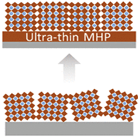
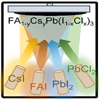
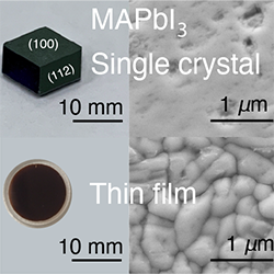
- A templating approach to controlling the growth of coevaporated halide perovskites
-
 | SY Yan, JB Patel, JE Lee, KA Elmestekawy, SR Ratnasingham, QM Yuan, LM Herz, NK Noel, MB Johnston
ACS Energy Lett., 8:4008–4015 (Oct 2023)
[
pdf ][ SI ][ ref ]
Metal halide perovskite semiconductors have shown significant potential for use in photovoltaic (PV) devices. While fabrication of perovskite thin films can be achieved through a variety of techniques, thermal vapor deposition is particularly promising, allowing for high-throughput fabrication. However, the ability to control the nucleation and growth of these materials, particularly at the charge transport layer/perovskite interface, is critical to unlocking the full potential of vapor-deposited perovskite PV. In this study, we explore the use of a templating layer to control the growth of coevaporated perovskite films and find that such templating leads to highly oriented films with identical morphology, crystal structure, and optoelectronic properties independent of the underlying layers. Solar cells incorporating templated FA(0.9)Cs(0.1)PbI(3-x)Cl(x) show marked improvements with steady-state power conversion efficiency over 19.8%. Our findings provide a straightforward and reproducible method of controlling the charge-transport layer/coevaporated perovskite interface, further clearing the path toward large-scale fabrication of efficient PV devices.
Citations: 24 (Scopus) 25 (Web of Science) |
- The 2023 terahertz science and technology roadmap
-
 | A Leitenstorfer, AS Moskalenko, T Kampfrath, J Kono, E Castro-camus, K Peng, N Qureshi, D Turchinovich, K Tanaka, AG Markelz, M Havenith, C Hough, HJ Joyce, MB Johnston, J Cunningham
J. Phys. D-Appl. Phys., 56:223001 (Jun 2023)
[
pdf ][ SI ][ ref ]
Terahertz (THz) radiation encompasses a wide spectral range within the electromagnetic spectrum that extends from microwaves to the far infrared (100 GHz-similar to 30 THz). Within its frequency boundaries exist a broad variety of scientific disciplines that have presented, and continue to present, technical challenges to researchers. During the past 50 years, for instance, the demands of the scientific community have substantially evolved and with a need for advanced instrumentation to support radio astronomy, Earth observation, weather forecasting, security imaging, telecommunications, non-destructive device testing and much more. Furthermore, applications have required an emergence of technology from the laboratory environment to production-scale supply and in-the-field deployments ranging from harsh ground-based locations to deep space. In addressing these requirements, the research and development community has advanced related technology and bridged the transition between electronics and photonics that high frequency operation demands. The multidisciplinary nature of THz work was our stimulus for creating the 2017 THz Science and Technology Roadmap (Dhillon et al 2017 J. Phys. D: Appl. Phys. 50 043001). As one might envisage, though, there remains much to explore both scientifically and technically and the field has continued to develop and expand rapidly. It is timely, therefore, to revise our previous roadmap and in this 2023 version we both provide an update on key developments in established technical areas that have important scientific and public benefit, and highlight new and emerging areas that show particular promise. The developments that we describe thus span from fundamental scientific research, such as THz astronomy and the emergent area of THz quantum optics, to highly applied and commercially and societally impactful subjects that include 6G THz communications, medical imaging, and climate monitoring and prediction. Our Roadmap vision draws upon the expertise and perspective of multiple international specialists that together provide an overview of past developments and the likely challenges facing the field of THz science and technology in future decades. The document is written in a form that is accessible to policy makers who wish to gain an overview of the current state of the THz art, and for the non-specialist and curious who wish to understand available technology and challenges. A such, our experts deliver a 'snapshot' introduction to the current status of the field and provide suggestions for exciting future technical development directions. Ultimately, we intend the Roadmap to portray the advantages and benefits of the THz domain and to stimulate further exploration of the field in support of scientific research and commercial realisation.
Citations: 426 (Scopus) 392 (Web of Science) |
- Narrowband, angle-tunable, helicity-dependent terahertz emission from nanowires of the topological dirac semimetal cd3as2
-
 | JL Boland, DA Damry, CQ Xia, P Schoenherr, D Prabhakaran, LM Herz, T Hesjedal, MB Johnston
ACS Photonics, 10:1473-1484 (Apr 2023)
[
pdf ][ SI ][ ref ]
All-optical control of terahertz pulses is essential for the development of optoelectronic devices for next-generation quantum technologies. Despite substantial research in THz generation methods, polarization control remains difficult. Here, we demonstrate that by exploiting band structure topology, both helicity-dependent and helicityindependent THz emission can be generated from nanowires of the topological Dirac semimetal Cd3As2. We show that narrowband THz pulses can be generated at oblique incidence by driving the system with optical (1.55 eV) pulses with circular polarization. Varying the incident angle also provides control of the peak emission frequency, with peak frequencies spanning 0.21-1.40 THz as the angle is tuned from 15 to 45 degrees. We therefore present Cd3As2 nanowires as a promising novel material platform for controllable terahertz emission.
|
- Synergistic surface modification of tin-lead perovskite solar cells
-
 | SF Hu, P Zhao, K Nakano, RDJ Oliver, J Pascual, JA Smith, T Yamada, MA Truong, R Murdey, N Shioya, T Hasegawa, M Ehara, MB Johnston, K Tajima, Y Kanemitsu, HJ Snaith, A Wakamiya
Adv. Mater., 35:2208320 (Mar 2023)
[
pdf ][ SI ][ ref ]
Interfaces in thin-film photovoltaics play a pivotal role in determining device efficiency and longevity. In this work, the top surface treatment of mixed tin-lead (approximate to 1.26 eV) halide perovskite films for p-i-n solar cells is studied. Charge extraction is promoted by treating the perovskite surface with piperazine. This compound reacts with the organic cations at the perovskite surface, modifying the surface structure and tuning the interfacial energy level alignment. In addition, the combined treatment with C-60 pyrrolidine tris-acid (CPTA) reduces hysteresis and leads to efficiencies up to 22.7%, with open-circuit voltage values reaching 0.90 V, approximate to 92% of the radiative limit for the bandgap of this material. The modified cells also show superior stability, with unencapsulated cells retaining 96% of their initial efficiency after >2000 h of storage in N-2 and encapsulated cells retaining 90% efficiency after >450 h of storage in air. Intriguingly, CPTA preferentially binds to Sn2+ sites at film surface over Pb2+ due to the energetically favored exposure of the former, according to first-principles calculations. This work provides new insights into the surface chemistry of perovskite films in terms of their structural, electronic, and defect characteristics and this knowledge is used to fabricate state-of-the-art solar cells.
Citations: 88 (Scopus) 87 (Web of Science) |
- Charge-carrier dynamics of solution-processed antimony- and bismuth-based chalcogenide thin films
-
 | ZL Jia, M Righetto, YJ Yang, CQ Xia, YY Li, RM Li, YW Li, B Yu, Y Liu, HM Huang, MB Johnston, LM Herz, QQ Lin
ACS Energy Lett., 8:1485-1492 (Feb 2023)
[
pdf ][ SI ][ ref ]
Chalcogenide-based semiconductors have recently emerged as promising candidates for optoelectronic devices, benefiting from their low-cost, solution processability, excellent stability and tunable optoelectronic properties. However, the understanding of their fundamental optoelectronic properties is far behind the success of device performance and starts to limit their further development. To fill this gap, we conduct a comparative study of chalcogenide absorbers across a wide material space, in order to assess their suitability for different types of applications. We utilize optical-pump terahertz-probe spectroscopy and time-resolved microwave conductivity techniques to fully analyze their charge-carrier dynamics. We show that antimony-based chalcogenide thin films exhibit relatively low charge-carrier mobilities and short lifetimes, compared with bismuth-based chalcogenides. In particular, AgBiS2 thin films possess the highest mobility, and Sb2S3 thin films have less energetic disorder, which are beneficial for photovoltaic devices. On the contrary, Bi(2)S(3 )showed ultralong carrier lifetime and high photoconductive gain, which is beneficial for designing photoconductors.
Citations: 44 (Scopus) 45 (Web of Science) |
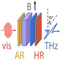
- Optimised spintronic emitters of terahertz radiation for time-domain spectroscopy
-
 | FM Wagner, S Melnikas, J Cramer, DA Damry, CQ Xia, K Peng, G Jakob, M Klaui, S Kicas, MB Johnston
J. Infrared Millim. Terahertz Waves, 44:52–65 (Jan 2023)
[
pdf ][ SI ][ ref ]
Spintronic metal thin films excited by femtosecond laser pulses have recently emerged as excellent broadband sources of terahertz (THz) radiation. Unfortunately, these emitters transmit a significant proportion of the incident excitation laser, which causes two issues: first, the transmitted light can interfere with measurements and so must be attenuated; second, the transmitted light is effectively wasted as it does not drive further THz generation. Here, we address both issues with the inclusion of a high-reflectivity (HR) coating made from alternating layers of SiO2 and Ta2O5. Emitters with the HR coating transmit less than 0.1% of the incident excitation pulse. Additionally, we find that the HR coating increases the peak THz signal by roughly 35%, whereas alternative attenuating elements, such as cellulose nitrate films, reduce the THz signal. To further improve the emission, we study the inclusion of an anti-reflective coating to the HR-coated emitters and find the peak THz signal is enhanced by a further 4%.
|
- Thermally stable perovskite solar cells by all-vacuum deposition
-
 | QM Yuan, KB Lohmann, RDJ Oliver, AJ Ramadan, SY Yan, JM Ball, MG Christoforo, NK Noel, HJ Snaith, LM Herz, MB Johnston
ACS Appl. Mater. Interfaces, 15:772-781 (Jan 2023)
[
pdf ][ SI ][ ref ]
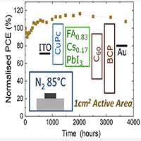
Vacuum deposition is a solvent-free method suitable for growing thin films of metal halide perovskite (MHP) semiconductors. However, most reports of high-efficiency solar cells based on such vacuum-deposited MHP films incorporate solution-processed hole transport layers (HTLs), thereby complicating prospects of industrial upscaling and potentially affecting the overall device stability. In this work, we investigate organometallic copper phthalocyanine (CuPc) and zinc phthalocyanine (ZnPc) as alternative, low-cost, and durable HTLs in all-vacuum-deposited solvent-free formamidinium-cesium lead triodide [CH(NH2)2]0.83Cs0.17PbI3 (FACsPbI3) perovskite solar cells. We elucidate that the CuPc HTL, when employed in an \"inverted\" p-i-n solar cell configuration, attains a solar-to-electrical power conversion efficiency of up to 13.9%. Importantly, unencapsulated devices as large as 1 cm2 exhibited excellent longterm stability, demonstrating no observable degradation in efficiency after more than 5000 h in storage and 3700 h under 85 degrees C thermal stressing in N2 atmosphere.
Citations: 35 (Scopus) 32 (Web of Science) |
- Intermediate-phase engineering via dimethylammonium cation additive for stable perovskite solar cells
-
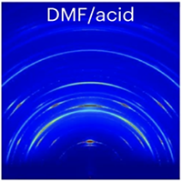 | DP McMeekin, P Holzhey, SO Funrer, SP Harvey, LT Schelhas, JM Ball, S Mahesh, S Seo, N Hawkins, JF Lu, MB Johnston, JJ Berry, U Bach, HJ Snaith
Nat. Mater., 22:73--83 (Jan 2023)
[
pdf ][ SI ][ ref ]
Achieving the long-term stability of perovskite solar cells is arguably the most important challenge required to enable widespread commercialization. Understanding the perovskite crystallization process and its direct impact on device stability is critical to achieving this goal. The commonly employed dimethyl-formamide/dimethyl-sulfoxide solvent preparation method results in a poor crystal quality and microstructure of the polycrystalline perovskite films. In this work, we introduce a high-temperature dimethyl-sulfoxide-free processing method that utilizes dimethylammonium chloride as an additive to control the perovskite intermediate precursor phases. By controlling the crystallization sequence, we tune the grain size, texturing, orientation (corner-up versus face-up) and crystallinity of the formamidinium (FA)/caesium (FA)(y)Cs1-yPb(IxBr1-x)(3) perovskite system. A population of encapsulated devices showed improved operational stability, with a median T80 lifetime (the time over which the device power conversion efficiency decreases to 80% of its initial value) for the steady-state power conversion efficiency of 1,190 hours, and a champion device showed a T80 of 1,410 hours, under simulated sunlight at 65 & DEG;C in air, under open-circuit conditions. This work highlights the importance of material quality in achieving the long-term operational stability of perovskite optoelectronic devices.
Citations: 199 (Scopus) 197 (Web of Science) |
- Impact of hole-transport layer and interface passivation on halide segregation in mixed-halide perovskites
-
 | VJY Lim, AJ Knight, RDJ Oliver, HJ Snaith, MB Johnston, LM Herz
Adv. Funct. Mater., 32:2204825 (Oct 2022)
[
pdf ][ SI ][ ref ]
Mixed-halide perovskites offer ideal bandgaps for tandem solar cells, but photoinduced halide segregation compromises photovoltaic device performance. This study explores the influence of a hole-transport layer, necessary for a full device, by monitoring halide segregation through in situ, concurrent X-ray diffraction and photoluminescence measurements to disentangle compositional and optoelectronic changes. This work demonstrates that top coating FA(0.83)Cs(0.17)Pb(Br0.4I0.6)(3) perovskite films with a poly(triaryl)amine (PTAA) hole-extraction layer surprisingly leads to suppression of halide segregation because photogenerated charge carriers are rapidly trapped at interfacial defects that do not drive halide segregation. However, the generation of iodide-enriched regions near the perovskite/PTAA interface enhances hole back-transfer from the PTAA layer through improved energy level offsets, increasing radiative recombination losses. It is further found that while passivation with a piperidinium salt slows halide segregation in perovskite films, the addition of a PTAA top-coating accelerates such effects, elucidating the specific nature of trap types that are able to drive the halide segregation process. This work highlights the importance of selective passivation techniques for achieving efficient and stable wide-bandgap perovskite photovoltaic devices.
Citations: 33 (Scopus) 34 (Web of Science) |
- Polarization anisotropy in nanowires: fundamental concepts and progress towards terahertz-band polarization devices
-
 | MB Johnston, HJ Joyce
Prog. Quantum Electron., 85:100417 (Aug 2022)
[
pdf ][ SI ][ ref ]
Pronounced polarization anisotropy in semiconductor nanowires has been exploited to achieve polarization-sensitive devices operating across the electromagnetic spectrum, from the ultraviolet to the terahertz band. This contribution describes the physical origins of optical and electrical anisotropy in nanowires. Polarization anisotropy arising from dielectric contrast, and the behaviour of (nano)wire grid polarizers, are derived from first principles. This review discusses experimental observations of polarization-sensitive light-matter interactions in nanowires. It then describes how these phenomena are employed in devices that detect or modulate polarized ter-ahertz radiation on ultrafast timescales. Such novel terahertz device concepts are expected to find use in a wide variety of applications including high-speed terahertz-band communications and molecular fingerprinting.
Citations: 18 (Scopus) 18 (Web of Science) |
- Controlling intrinsic quantum confinement in formamidinium lead triiodide perovskite through cs substitution
-
 | KA Elmestekawy, AD Wright, KB Lohmann, J Borchert, MB Johnston, LM Herz
ACS Nano, 16:9640-9650 (Jun 2022)
[
pdf ][ SI ][ ref ]
Lead halide perovskites are leading candidates for photovoltaic and light-emitting devices, owing to their excellent and widely tunable optoelectronic properties. Nanostructure control has been central to their development, allowing for improvements in efficiency and stability, and changes in electronic dimensionality. Recently, formamidinium lead triiodide (FAPbI3) has been shown to exhibit intrinsic quantum confinement effects in nominally bulk thin films, apparent through above-bandgap absorption peaks. Here, we show that such nanoscale electronic effects can be controlled through partial replacement of the FA cation with Cs. We find that Cs-cation exchange causes a weakening of quantum confinement in the perovskite, arising from changes in the bandstructure, the length scale of confinement, or the presence of delta H-phase electronic barriers. We further observe photon emission from quantum-confined regions, highlighting their potential usefulness to light-emitting devices and single-photon sources. Overall, controlling this intriguing quantum phenomenon will allow for its suppression or enhancement according to need.
Citations: 20 (Scopus) 19 (Web of Science) |
- Solvent-Free Method for Defect Reduction and Improved Performance of {p-i-n} Vapor-Deposited Perovskite Solar Cells
-
 | KB Lohmann, SG Motti, RDJ Oliver, AJ Ramadan, HC Sansom, QM Yuan, KA Elmestekawy, JB Patel, JM Ball, LM Herz, HJ Snaith, MB Johnston
ACS Energy Lett., 7:1903-1911 (May 2022)
[
pdf ][ SI ][ ref ]
As perovskite-based photovoltaics near commercialization, it is imperative to develop industrial-scale defect-passivation techniques. Vapor deposition is a solvent-free fabrication technique that is widely implemented in industry and can be used to fabricate metal-halide perovskite thin films. We demonstrate markably improved growth and optoelectronic properties for vapor-deposited [CH(NH2)2]0.83Cs0.17PbI3 perovskite solar cells by partially substituting PbI2 for PbCl2 as the inorganic precursor. We find the partial substitution of PbI2 for PbCl2 enhances photoluminescence lifetimes from 5.6 ns to over 100 ns, photoluminescence quantum yields by more than an order of magnitude, and charge-carrier mobility from 46 cm2/(V s) to 56 cm2/(V s). This results in improved solar-cell power conversion efficiency, from 16.4\% to 19.3\% for the devices employing perovskite films deposited with 20\% substitution of PbI2 for PbCl2. Our method presents a scalable, dry, and solvent-free route to reducing nonradiative recombination centers and hence improving the performance of vapor-deposited metal-halide perovskite solar cells.
Citations: 85 (Scopus) 82 (Web of Science) |
- Optoelectronic Properties of Mixed Iodide--Bromide Perovskites from First-Principles Computational Modeling and Experiment
-
 | Y Chen, SG Motti, RDJ Oliver, AD Wright, HJ Snaith, MB Johnston, LM Herz, MR Filip
J. Phys. Chem. Lett., 13:4184-4192 (May 2022)
[
pdf ][ SI ][ ref ]
Halogen mixing in lead-halide perovskites is an effective route for tuning the band gap in light emission and multijunction solar cell applications. Here we report the effect of halogen mixing on the optoelectronic properties of lead-halide perovskites from theory and experiment. We applied the virtual crystal approximation within density functional theory, the GW approximation, and the Bethe–Salpeter equation to calculate structural, vibrational, and optoelectronic properties for a series of mixed halide perovskites. We separately perform spectroscopic measurements of these properties and analyze the impact of halogen mixing on quasiparticle band gaps, effective masses, absorption coefficients, charge-carrier mobilities, and exciton binding energies. Our joint theoretical–experimental study demonstrates that iodide–bromide mixed-halide perovskites can be modeled as homovalent alloys, and local structural distortions do not play a significant role for the properties of these mixed species. Our study outlines a general theoretical–experimental framework for future investigations of novel chemically mixed systems.
Citations: 29 (Scopus) 29 (Web of Science) |
- Air-degradation mechanisms in mixed lead-tin halide perovskites for solar cells
-
 | VJY Lim, AM Ulatowski, C Kamaraki, MT Klug, LM Perez, MB Johnston, LM Herz
Adv. Energy Mater., 0:2200847 (May 2022)
[
pdf ][ SI ][ ref ]
Owing to the bandgap-bowing effect, mixed lead-tin halide perovskites provide ideal bandgaps for the bottom subcell of all-perovskite tandem photovoltaic devices that offer fundamentally elevated power-conversion efficiencies. However, these materials suffer from degradation in ambient air, which worsens their optoelectronic properties and hinders their usability for photovoltaic applications. Such degradation pathways are not yet fully understood, especially for the perovskites in the middle of the APb(x)Sn(1-x)I(3) solid solution line, which offer the narrowest bandgaps across the range. This study unravels the degradation mechanisms of APb(x)Sn(1-x)I(3) perovskites, reporting clear differences between mixed lead-tin (x = 0.5) and tin-only (x = 0) perovskites. The dynamic optoelectronic properties, electronic structure, crystal structure, and decomposition products of the perovskite thin films are examined in situ during air exposure. Both perovskite compositions suffer from the formation of defects over the timescale of hours, as indicated by a significant reduction in their charge-carrier diffusion lengths. For tin-only perovskite, degradation predominantly causes the formation of energetically shallow tin vacancies and hole doping. However, for mixed lead-tin perovskite, deep trap states are formed that significantly accelerate charge-carrier recombination, yet leave mobilities relatively unaffected. These findings highlight the need for passivation strategies tailored specifically to mixed lead-tin iodide perovskites.
Citations: 45 (Scopus) 51 (Web of Science) |
- Interplay of structure, charge-carrier localization and dynamics in copper-silver-bismuth-halide semiconductors
-
 | LRV Buizza, HC Sansom, AD Wright, AM Ulatowski, MB Johnston, HJ Snaith, LM Herz
Adv. Funct. Mater., 32:2108392 (Feb 2022)
[
pdf ][ SI ][ ref ]
Silver-bismuth based semiconductors represent a promising new class of materials for optoelectronic applications because of their high stability, all-inorganic composition, and advantageous optoelectronic properties. In this study, charge-carrier dynamics and transport properties are investigated across five compositions along the AgBiI4-CuI solid solution line (stoichiometry Cu-4x(AgBi)(1-x)I-4). The presence of a close-packed iodide sublattice is found to provide a good backbone for general semiconducting properties across all of these materials, whose optoelectronic properties are found to improve markedly with increasing copper content, which enhances photoluminescence intensity and charge-carrier transport. Photoluminescence and photoexcitation-energy-dependent terahertz photoconductivity measurements reveal that this enhanced charge-carrier transport derives from reduced cation disorder and improved electronic connectivity owing to the presence of Cu+. Further, increased Cu+ content enhances the band curvature around the valence band maximum, resulting in lower charge-carrier effective masses, reduced exciton binding energies, and higher mobilities. Finally, ultrafast charge-carrier localization is observed upon pulsed photoexcitation across all compositions investigated, lowering the charge-carrier mobility and leading to Langevin-like bimolecular recombination. This process is concluded to be intrinsically linked to the presence of silver and bismuth, and strategies to tailor or mitigate the effect are proposed and discussed.
Citations: 39 (Scopus) 40 (Web of Science) |
- The application of one-dimensional nanostructures in terahertz frequency devices
-
 | K Peng, MB Johnston
Appl. Phys. Rev., 8:041314 (Dec 2021)
[
pdf ][ SI ][ ref ]
One-dimensional nanostructures commonly refer to nanomaterials with a large length-to-diameter ratio, such as nanowires, nanotubes, nanorods, and nanopillars. The nanoscale lateral dimensions and high aspect ratios of these (quasi) one-dimensional nanostructures result in fascinating optical and electrical properties, including strongly anisotropic optical absorption, controlled directionality of light emission, confined charge-carrier transport and/or ballistic transport, which make one-dimensional nanostructures ideal building blocks for applications in highly integrated photonic, electronic, and optoelectronic systems. In this article, we review recent developments of very high (terahertz) frequency devices based on these one-dimensional nanostructures, particularly focusing on carbon nanotubes and semiconductor nanowires. We discuss state-of-the-art nanomaterials synthesis, device-fabrication techniques, device-operating mechanisms, and device performance. The combination of nanotechnology and terahertz science is a nascent research field which has created advanced THz sources, detectors, and modulators, leading to terahertz systems with extended functionalities. The goal of this article is to present the up-to-date worldwide status of this field and to highlight the current challenges and future opportunities.
Citations: 37 (Scopus) 33 (Web of Science) |
- Phase segregation in mixed-halide perovskites affects charge-carrier dynamics while preserving mobility
-
 | SG Motti, JB Patel, RDJ Oliver, HJ Snaith, MB Johnston, LM Herz
Nat. Commun., 12:6955 (Nov 2021)
[
pdf ][ SI ][ ref ]
Mixed halide perovskites can provide optimal bandgaps for tandem solar cells which are key to improved cost-efficiencies, but can still suffer from detrimental illumination-induced phase segregation. Here we employ optical-pump terahertz-probe spectroscopy to investigate the impact of halide segregation on the charge-carrier dynamics and transport properties of mixed halide perovskite films. We reveal that, surprisingly, halide segregation results in negligible impact to the THz charge-carrier mobilities, and that charge carriers within the I-rich phase are not strongly localised. We further demonstrate enhanced lattice anharmonicity in the segregated I-rich domains, which is likely to support ionic migration. These phonon anharmonicity effects also serve as evidence of a remarkably fast, picosecond charge funnelling into the narrow-bandgap I-rich domains. Our analysis demonstrates how minimal structural transformations during phase segregation have a dramatic effect on the charge-carrier dynamics as a result of charge funnelling. We suggest that because such enhanced recombination is radiative, performance losses may be mitigated by deployment of careful light management strategies in solar cells. Phase segregation in mixed halide perovskite is known to alter the optoelectronic properties, but how it affects charge carriers is not clear. Here, the authors use THz spectroscopy to reveal that high carrier mobilities are well preserved, while recombination dynamics is affected by charge funnelling upon segregation.
Citations: 164 (Scopus) 170 (Web of Science) |
- Ultrafast photo-induced phonon hardening due to pauli blocking in {MAPbI}$_3$ single-crystal and polycrystalline perovskites
-
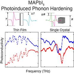 | CQ Xia, S Ponce, JL Peng, AM Ulatowski, JB Patel, AD Wright, RL Milot, H Kraus, QQ Lin, LM Herz, F Giustino, MB Johnston
J. Phys-Mater., 4:044017 (Oct 2021)
[
pdf ][ SI ][ ref ]
Metal-halide perovskite semiconductors have attracted intense interest over the past decade, particularly for applications in photovoltaics. Low-energy optical phonons combined with significant crystal anharmonicity play an important role in charge-carrier cooling and scattering in these materials, strongly affecting their optoelectronic properties. We have observed optical phonons associated with Pb-I stretching in both MAPbI(3) single crystals and polycrystalline thin films as a function of temperature by measuring their terahertz conductivity spectra with and without photoexcitation. An anomalous bond hardening was observed under above-bandgap illumination for both single-crystal and polycrystalline MAPbI(3). First-principles calculations reproduced this photo-induced bond hardening and identified a related lattice contraction (photostriction), with the mechanism revealed as Pauli blocking. For single-crystal MAPbI(3), phonon lifetimes were significantly longer and phonon frequencies shifted less with temperature, compared with polycrystalline MAPbI(3). We attribute these differences to increased crystalline disorder, associated with grain boundaries and strain in the polycrystalline MAPbI(3). Thus we provide fundamental insight into the photoexcitation and electron-phonon coupling in MAPbI(3).
|
- Revealing ultrafast charge-carrier thermalization in tin-iodide perovskites through novel pump-push-probe terahertz spectroscopy
-
 | AM Ulatowski, MD Farrar, HJ Snaith, MB Johnston, LM Herz
ACS Photonics, 8:2509-2518 (Aug 2021)
[
pdf ][ SI ][ ref ]
Tin-iodide perovskites are an important group of semiconductors for photovoltaic applications, promising higher intrinsic charge-carrier mobilities and lower toxicity than their lead-based counterparts. Controllable tin vacancy formation and the ensuing hole doping provide interesting opportunities to investigate dynamic intraband transitions of charge carriers in these materials. Here, we present for the first time an experimental implementation of a novel Optical-Pump-IR-Push-THz-Probe spectroscopic technique and demonstrate its suitability to investigate the intraband relaxation dynamics of charge carriers brought into nonequilibrium by an infrared \"push\" pulse. We observe a push-induced decrease of terahertz conductivity for both chemically- and photodoped FA(0.83)Cs(0.17)SnI(3) thin films and show that these effects derive from stimulated THz emission. We use this technique to reveal that newly photogenerated charge carriers relax within the bands of FA(0.83)Cs(0.17)SnI(3) on a subpicosecond time scale when a large, already fully thermalized (cold) population of charge-carriers is present. Such rapid dissipation of the initial charge-carrier energy suggests that the propensity of tin halide perovskites toward unintentional self-doping resulting from tin vacancy formation makes these materials less suited to implementation in hot-carrier solar cells than their lead-based counterparts.
Citations: 23 (Scopus) 24 (Web of Science) |
- Hot electron cooling in InSb probed by ultrafast time-resolved terahertz cyclotron resonance
-
 | CQ Xia, M Monti, JL Boland, LM Herz, J Lloyd-hughes, MR Filip, MB Johnston
Phys. Rev. B, 103:245205 (Jun 2021)
[
pdf ][ SI ][ ref ]
Measuring terahertz (THz) conductivity on an ultrafast timescale is an excellent way to observe charge-carrier dynamics in semiconductors as a function of time after photoexcitation. However, a conductivity measurement alone cannot separate the effects of charge-carrier recombination from effective mass changes as charges cool and experience different regions of the electronic band structure. Here we present a form of time-resolved magneto-THz spectroscopy that allows us to measure cyclotron effective mass on a picosecond timescale. We demonstrate this technique by observing electron cooling in the technologically significant narrow-bandgap semiconductor indium antimonide. A significant reduction of electron effective mass from 0.032 to 0.017 m(e) is observed in the first 200 ps after injecting hot electrons. The measured electron effective mass in InSb as a function of photoinjected electron density agrees well with conduction band nonparabolicity predictions from ab initio calculations of the quasiparticle band structure.
Citations: 15 (Scopus) 13 (Web of Science) |
- Charge-carrier mobility and localization in semiconducting {Cu}$_2${AgBiI}$_6$ for photovoltaic applications
-
 | LRV Buizza, AD Wright, G Longo, HC Sansom, CQ Xia, MJ Rosseinsky, MB Johnston, HJ Snaith, LM Herz
ACS Energy Lett., 6:1729-1739 (May 2021)
[
pdf ][ SI ][ ref ]
Lead-free silver-bismuth semiconductors have become increasingly popular materials for optoelectronic applications, building upon the success of lead halide perovskites. In these materials, charge-lattice couplings fundamentally determine charge transport, critically affecting device performance. In this study, we investigate the optoelectronic properties of the recently discovered lead-free semiconductor Cu2AgBiI6 using temperature-dependent photoluminescence, absorption, and optical-pump terahertz-probe spectroscopy. We report ultrafast charge-carrier localization effects, evident from sharp THz photoconductivity decays occurring within a few picoseconds after excitation and a rise in intensity with decreasing temperature of long-lived, highly Stokes-shifted photoluminescence. We conclude that charge carriers in Cu2AgBiI6 are subject to strong charge-lattice coupling. However, such small polarons still exhibit mobilities in excess of 1 cm(2) V-1 s(-1) at room temperature because of low energetic barriers to formation and transport. Together with a low exciton binding energy of similar to 29 meV and a direct band gap near 2.1 eV, these findings highlight Cu2AgBiI6 as an attractive lead-free material for photovoltaic applications.
Citations: 72 (Scopus) 73 (Web of Science) |
- Ultrafast excited-state localization in Cs$_2$AgBiBr$_6$ double perovskite
-
 | AD Wright, LRV Buizza, KJ Savill, G Longo, HJ Snaith, MB Johnston, LM Herz
J. Phys. Chem. Lett., 12:3352-3360 (Apr 2021)
[
pdf ][ SI ][ ref ]
Cs2AgBiBr6 is a promising metal halide double perovskite offering the possibility of efficient photovoltaic devices based on lead-free materials. Here, we report on the evolution of photoexcited charge carriers in Cs2AgBiBr6 using a combination of temperature-dependent photoluminescence, absorption and optical pump-terahertz probe spectroscopy. We observe rapid decays in terahertz photoconductivity transients that reveal an ultrafast, barrier-free localization of free carriers on the time scale of 1.0 ps to an intrinsic small polaronic state. While the initially photogenerated delocalized charge carriers show bandlike transport, the self-trapped, small polaronic state exhibits temperature-activated mobilities, allowing the mobilities of both to still exceed 1 cm(2) V-1 s(-1) at room temperature. Self-trapped charge carriers subsequently diffuse to color centers, causing broad emission that is strongly red-shifted from a direct band edge whose band gap and associated exciton binding energy shrink with increasing temperature in a correlated manner. Overall, our observations suggest that strong electron-phonon coupling in this material induces rapid charge-carrier localization.
Citations: 143 (Scopus) 145 (Web of Science) |
- Limits to electrical mobility in lead-halide perovskite semiconductors
-
 | CQ Xia, JL Peng, S Ponce, JB Patel, AD Wright, TW Crothers, MU Rothmann, J Borchert, RL Milot, H Kraus, QQ Lin, F Giustino, LM Herz, MB Johnston
J. Phys. Chem. Lett., 12:3607-3617 (Apr 2021)
[
pdf ][ SI ][ ref ]
Semiconducting polycrystalline thin films are cheap to produce and can be deposited on flexible substrates, yet high-performance electronic devices usually utilize single-crystal semiconductors, owing to their superior charge-carrier mobilities and longer diffusion lengths. Here we show that the electrical performance of polycrystalline films of metal-halide perovskites (MHPs) approaches that of single crystals at room temperature. Combining temperature-dependent terahertz conductivity measurements and ab initio calculations we uncover a complete picture of the origins of charge-carrier scattering in single crystals and polycrystalline films of CH3NH3PbI3. We show that Frohlich scattering of charge carriers with multiple phonon modes is the dominant mechanism limiting mobility, with grain-boundary scattering further reducing mobility in polycrystalline films. We reconcile the large discrepancy in charge-carrier diffusion lengths between single crystals and films by considering photon reabsorption. Thus, polycrystalline films of MHPs offer great promise for devices beyond solar cells, including light-emitting diodes and modulators.
Citations: 86 (Scopus) 83 (Web of Science) |
- Crystallization of cspbbr3 single crystals in water for x-ray detection
-
 | JL Peng, CQ Xia, YL Xu, RM Li, LH Cui, JK Clegg, LM Herz, MB Johnston, QQ Lin
Nat. Commun., 12:1531 (Mar 2021)
[
pdf ][ SI ][ ref ]
Metal halide perovskites have fascinated the research community over the past decade, and demonstrated unprecedented success in optoelectronics. In particular, perovskite single crystals have emerged as promising candidates for ionization radiation detection, due to the excellent opto-electronic properties. However, most of the reported crystals are grown in organic solvents and require high temperature. In this work, we develop a low-temperature crystallization strategy to grow CsPbBr3 perovskite single crystals in water. Then, we carefully investigate the structure and optoelectronic properties of the crystals obtained, and compare them with CsPbBr3 crystals grown in dimethyl sulfoxide. Interestingly, the water grown crystals exhibit a distinct crystal habit, superior charge transport properties and better stability in air. We also fabricate X-ray detectors based on the CsPbBr3 crystals, and systematically characterize their device performance. The crystals grown in water demonstrate great potential for X-ray imaging with enhanced performance metrics. Perovskite single crystals are commonly grown in organic solvents, which require relatively high temperature condition. Here, the authors develop a low-temperature crystallisation strategy to grow CsPbBr3 single crystals in water with improved charge transport properties and stability.
Citations: 296 (Scopus) 292 (Web of Science) |
- Halide segregation in mixed-halide perovskites: influence of a-site cations
-
 | AJ Knight, J Borchert, RDJ Oliver, JB Patel, PG Radaelli, HJ Snaith, MB Johnston, LM Herz
ACS Energy Lett., 6:799-808 (Feb 2021)
[
pdf ][ SI ][ ref ]
Mixed-halide perovskites offer bandgap tunability essential for multijunction solar cells; however, a detrimental halide segregation under light is often observed. Here we combine simultaneous in situ photoluminescence and X-ray diffraction measurements to demonstrate clear differences in compositional and optoelectronic changes associated with halide segregation in MAPb(Br0.5I0.5)(3) and FA(0.83)Cs(0.17)Pb(Br0.4I0.6)(3) films. We report evidence for low-barrier ionic pathways in MAPb(Br0.5I0.5)(3), which allow for the rearrangement of halide ions in localized volumes of perovskite without significant compositional changes to the bulk material. In contrast, FA(0.83)Cs(0.17)Pb(Br0.4I0.6)(3) lacks such low-barrier ionic pathways and is, consequently, more stable against halide segregation. However, under prolonged illumination, it exhibits a considerable ionic rearrangement throughout the bulk material, which may be triggered by an initial demixing of A-site cations, altering the composition of the bulk perovskite and reducing its stability against halide segregation. Our work elucidates links between composition, ionic pathways, and halide segregation, and it facilitates the future engineering of phase-stable mixed-halide perovskites.
Citations: 220 (Scopus) 217 (Web of Science) |
- Nanotechnology for catalysis and solar energy conversion
-
 | U Banin, N Waiskopf, L Hammarstrom, G Boschloo, M Freitag, EMJ Johansson, J Sa, H Tian, MB Johnston, LM Herz, RL Milot, MG Kanatzidis, W Ke, I Spanopoulos, KL Kohlstedt, GC Schatz, N Lewis, T Meyer, AJ Nozik, MC Beard
Nanotechnology, 32:042003 (Jan 2021)
[
pdf ][ SI ][ ref ]
This roadmap on Nanotechnology for Catalysis and Solar Energy Conversion focuses on the application of nanotechnology in addressing the current challenges of energy conversion: \'high efficiency, stability, safety, and the potential for low-cost/scalable manufacturing\' to quote from the contributed article by Nathan Lewis. This roadmap focuses on solar-to-fuel conversion, solar water splitting, solar photovoltaics and bio-catalysis. It includes dye-sensitized solar cells (DSSCs), perovskite solar cells, and organic photovoltaics. Smart engineering of colloidal quantum materials and nanostructured electrodes will improve solar-to-fuel conversion efficiency, as described in the articles by Waiskopf and Banin and Meyer. Semiconductor nanoparticles will also improve solar energy conversion efficiency, as discussed by Boschloo et al in their article on DSSCs. Perovskite solar cells have advanced rapidly in recent years, including new ideas on 2D and 3D hybrid halide perovskites, as described by Spanopoulos et al \'Next generation\' solar cells using multiple exciton generation (MEG) from hot carriers, described in the article by Nozik and Beard, could lead to remarkable improvement in photovoltaic efficiency by using quantization effects in semiconductor nanostructures (quantum dots, wires or wells). These challenges will not be met without simultaneous improvement in nanoscale characterization methods. Terahertz spectroscopy, discussed in the article by Milot et al is one example of a method that is overcoming the difficulties associated with nanoscale materials characterization by avoiding electrical contacts to nanoparticles, allowing characterization during device operation, and enabling characterization of a single nanoparticle. Besides experimental advances, computational science is also meeting the challenges of nanomaterials synthesis. The article by Kohlstedt and Schatz discusses the computational frameworks being used to predict structure-property relationships in materials and devices, including machine learning methods, with an emphasis on organic photovoltaics. The contribution by Megarity and Armstrong presents the \'electrochemical leaf\' for improvements in electrochemistry and beyond. In addition, biohybrid approaches can take advantage of efficient and specific enzyme catalysts. These articles present the nanoscience and technology at the forefront of renewable energy development that will have significant benefits to society.
Citations: 74 (Scopus) 53 (Web of Science) |
- Understanding dark current-voltage characteristics in metal-halide perovskite single crystals
-
 | EA Duijnstee, MB Johnston, LJA Koster, JC Lim, HJ Snaith
Phys. Rev. Appl., 15:014006 (Jan 2021)
[
pdf ][ SI ][ ref ]
Hybrid halide perovskites have great potential for application in optoelectronic devices. However, an understanding of some basic properties, such as charge-carrier transport, remains inconclusive, mainly due to the mixed ionic and electronic nature of these materials. Here, we perform temperature-dependent pulsed-voltage space-charge-limited current measurements to provide a detailed look into the electronic properties of methylammonium lead tribromide (MAPbBr(3)) and methylammonium lead triiodide (MAPbI(3)) single crystals. We show that the background carrier density in these crystals is orders of magnitude higher than that expected from thermally excited carriers from the valence band. We highlight the complexity of the system via a combination of experiments and drift-diffusion simulations and show that different factors, such as thermal injection from the electrodes, temperature-dependent mobility, and trap and ion density, influence the free-carrier concentration. We experimentally determine effective activation energies for conductivity of (349 +/- 10) meV for MAPbBr3 and (193 +/- 12) meV for MAPbI(3), which includes the sum of all of these factors. We point out that fitting the dark current density-voltage curve with a drift-diffusion model allows for the extraction of intrinsic parameters, such as mobility and trap and ion density. From simulations, we determine a charge-carrier mobility of 12.9 cm(2)/Vs, a trap density of 1.52 x 10(13) cm(-3), and an ion density of 3.19 x 10(12) cm(-3) for MAPbBr(3) single crystals. Insights into charge-carrier transport in metal-halide perovskite single crystals will be beneficial for device optimization in various optoelectronic applications.
Citations: 59 (Scopus) 56 (Web of Science) |
- Terahertz conductivity analysis for highly doped thin-film semiconductors
-
 | AM Ulatowski, LM Herz, MB Johnston
J. Infrared Millim. Terahertz Waves, 41:1431-1449 (Dec 2020)
[
pdf ][ SI ][ ref ]
The analysis of terahertz transmission through semiconducting thin films has proven to be an excellent tool for investigating optoelectronic properties of novel materials. Terahertz time-domain spectroscopy (THz-TDS) can provide information about phonon modes of the crystal, as well as the electrical conductivity of the sample. When paired with photoexcitation, optical-pump-THz-probe (OPTP) technique can be used to gain an insight into the transient photoconductivity of the semiconductor, revealing the dynamics and the mobility of photoexcited charge carriers. As the relation between the conductivity of the material and the THz transmission function is generally complicated, simple analytical expressions have been developed to enable straightforward calculations of frequency-dependent conductivity from THz-TDS data in the regime of optically thin samples. Here, we assess the accuracy of these approximated analytical formulas in thin films of highly doped semiconductors, finding significant deviations of the calculated photoconductivity from its actual value in materials with background conductivity comparable to 10(2)omega(- 1)cm(- 1). We propose an alternative analytical expression, which greatly improves the accuracy of the estimated value of the real photoconductivity, while remaining simple to implement experimentally. Our approximation remains valid in thin films with high dark conductivity of up to 10(4)omega(- 1)cm(- 1)and provides a very high precision for calculating photoconductivity up to 10(4)omega(- 1)cm(- 1), and therefore is highly relevant for studies of photoexcited charge-carrier dynamics in electrically doped semiconductors. Using the example of heavily doped thin films of tin-iodide perovskites, we show a simple experimental method of implementing our correction and find that the commonly used expression for photoconductivity could result in an underestimate of charge-carrier mobility by over 50\%.
Citations: 56 (Scopus) 54 (Web of Science) |
- Impact of tin fluoride additive on the properties of mixed tin-lead iodide perovskite semiconductors
-
 | KJ Savill, AM Ulatowski, MD Farrar, MB Johnston, HJ Snaith, LM Herz
Adv. Funct. Mater., 30:2005594 (Dec 2020)
[
pdf ][ SI ][ ref ]
Mixed tin-lead halide perovskites are promising low-bandgap absorbers for all-perovskite tandem solar cells that offer higher efficiencies than single-junction devices. A significant barrier to higher performance and stability is the ready oxidation of tin, commonly mitigated by various additives whose impact is still poorly understood for mixed tin-lead perovskites. Here, the effects of the commonly used SnF(2)additive are revealed for FA(0)(.)(83)Cs(0)(.)(17)Sn(x)Pb(1-)(x)I(3)perovskites across the full compositional lead-tin range and SnF(2)percentages of 0.1-20\% of precursor tin content. SnF(2)addition causes a significant reduction in the background hole density associated with tin vacancies, yielding longer photoluminescence lifetimes, decreased energetic disorder, reduced Burstein-Moss shifts, and higher charge-carrier mobilities. Such effects are optimized for SnF(2)addition of 1%, while for 5% SnF(2)and above, additional nonradiative recombination pathways begin to appear. It is further found that the addition of SnF(2)reduces a tetragonal distortion in the perovskite structure deriving from the presence of tin vacancies that cause strain, particularly for high tin content. The optical phonon response associated with inorganic lattice vibrations is further explored, exhibiting a shift to higher frequency and significant broadening with increasing tin fraction, in accordance with lower effective atomic metal masses and shorter phonon lifetimes.
Citations: 92 (Scopus) 91 (Web of Science) |
- Intrinsic quantum confinement in formamidinium lead triiodide perovskite
-
 | AD Wright, G Volonakis, J Borchert, CL Davies, F Giustino, MB Johnston, LM Herz
Nat. Mater., 19:1201 (Nov 2020)
[
pdf ][ SI ][ ref ]
Understanding the electronic energy landscape in metal halide perovskites is essential for further improvements in their promising performance in thin-film photovoltaics. Here, we uncover the presence of above-bandgap oscillatory features in the absorption spectra of formamidinium lead triiodide thin films. We attribute these discrete features to intrinsically occurring quantum confinement effects, for which the related energies change with temperature according to the inverse square of the intrinsic lattice parameter, and with peak index in a quadratic manner. By determining the threshold film thickness at which the amplitude of the peaks is appreciably decreased, and through ab initio simulations of the absorption features, we estimate the length scale of confinement to be 10-20 nm. Such absorption peaks present a new and intriguing quantum electronic phenomenon in a nominally bulk semiconductor, offering intrinsic nanoscale optoelectronic properties without necessitating cumbersome additional processing steps. Oscillatory features in the absorption spectra of formamidinium lead triiodide perovskite thin films reveal the occurrence of intrinsic quantum confinement effects with confinement on the scale of tens of nanometres.
Citations: 48 (Scopus) 45 (Web of Science) |
- Efficient energy transfer mitigates parasitic light absorption in molecular charge-extraction layers for perovskite solar cells
-
 | HJ Eggimann, JB Patel, MB Johnston, LM Herz
Nat. Commun., 11:5525 (Nov 2020)
[
pdf ][ SI ][ ref ]
Organic semiconductors are commonly used as charge-extraction layers in metal-halide perovskite solar cells. However, parasitic light absorption in the sun-facing front molecular layer, through which sun light must propagate before reaching the perovskite layer, may lower the power conversion efficiency of such devices. Here, we show that such losses may be eliminated through efficient excitation energy transfer from a photoexcited polymer layer to the underlying perovskite. Experimentally observed energy transfer between a range of different polymer films and a methylammonium lead iodide perovskite layer was used as basis for modelling the efficacy of the mechanism as a function of layer thickness, photoluminescence quantum efficiency and absorption coefficient of the organic polymer film. Our findings reveal that efficient energy transfer can be achieved for thin (<= 10 nm) organic charge-extraction layers exhibiting high photoluminescence quantum efficiency. We further explore how the morphology of such thin polymer layers may be affected by interface formation with the perovskite.
Citations: 32 (Scopus) 31 (Web of Science) |
- Thermally stable passivation toward high efficiency inverted perovskite solar cells
-
 | RDJ Oliver, YH Lin, AJ Horn, CQ Xia, JH Warby, MB Johnston, AJ Ramadan, HJ Snaith
ACS Energy Lett., 5:3336-3343 (Nov 2020)
[
pdf ][ SI ][ ref ]
Although metal halide perovskite photovoltaics have shown an unprecedented rise in power conversion efficiency (PCE), they remain far from their theoretical PCE limit. Among the highest efficiencies to date are delivered when polycrystalline films are enhanced via \"molecular passivation\", but this can introduce new instabilities, in particular under severe accelerated aging conditions (e.g., at 85 degrees C in the dark or under full spectrum simulated sunlight). Here, we utilize a benzylammonium bromide passivation treatment to improve device performance, achieving the champion stabilized power output (SPO) of 19.5 \% in a p-i-n device architecture. We correlate the improved device performance with a significant increase in charge carrier diffusion lengths, mobilities, and lifetimes. Furthermore, treated devices maintain an increased performance during 120 h combined stressing under simulated full spectrum sunlight at 85 degrees C, indicating that enhancement from this passivation treatment is sustained under harsh accelerated aging conditions. This is a crucial step toward real-world operation-relevant passivation treatments.
Citations: 22 (Scopus) 22 (Web of Science) |
- Atomic-scale microstructure of metal halide perovskite
-
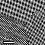 | MU Rothmann, JS Kim, J Borchert, KB Lohmann, CM O'Leary, AA Sheader, L Clark, HJ Snaith, MB Johnston, PD Nellist, LM Herz
Science, 370:eabb5940 (Oct 2020)
[
pdf ][ SI ][ ref ]
Hybrid organic-inorganic perovskites have high potential as materials for solar energy applications, but their microscopic properties are still not well understood. Atomic-resolution scanning transmission electron microscopy has provided invaluable insights for many crystalline solar cell materials, and we used this method to successfully image formamidinium lead triiodide [CH(NH2)(2)Pbl(3)] thin films with a low dose of electron irradiation. Such images reveal a highly ordered atomic arrangement of sharp grain boundaries and coherent perovskite/Pbl(2) interfaces, with a striking absence of long-range disorder in the crystal. We found that beam-induced degradation of the perovskite leads to an initial loss of formamidinium [CH(NH2)(2)] ions, leaving behind a partially unoccupied perovskite lattice, which explains the unusual regenerative properties of these materials. We further observed aligned point defects and climb-dissociated dislocations. Our findings thus provide an atomic-level understanding of technologically important lead halide perovskites.
Citations: 104 (Scopus) 282 (Web of Science) |
- Charge-carrier trapping and radiative recombination in metal halide perovskite semiconductors
-
 | MJ Trimpl, AD Wright, K Schutt, LRV Buizza, ZP Wang, MB Johnston, HJ Snaith, P Muller-buschbaum, LM Herz
Adv. Funct. Mater., 30:2004312 (Oct 2020)
[
pdf ][ SI ][ ref ]
Trap-related charge-carrier recombination fundamentally limits the performance of perovskite solar cells and other optoelectronic devices. While improved fabrication and passivation techniques have reduced trap densities, the properties of trap states and their impact on the charge-carrier dynamics in metal-halide perovskites are still under debate. Here, a unified model is presented of the radiative and nonradiative recombination channels in a mixed formamidinium-cesium lead iodide perovskite, including charge-carrier trapping, de-trapping and accumulation, as well as higher-order recombination mechanisms. A fast initial photoluminescence (PL) decay component observed after pulsed photogeneration is demonstrated to result from rapid localization of free charge carriers in unoccupied trap states, which may be followed by de-trapping, or nonradiative recombination with free carriers of opposite charge. Such initial decay components are shown to be highly sensitive to remnant charge carriers that accumulate in traps under pulsed-laser excitation, with partial trap occupation masking the trap density actually present in the material. Finally, such modelling reveals a change in trap density at the phase transition, and disentangles the radiative and nonradiative charge recombination channels present in FA(0.95)Cs(0.05)PbI(3,)accurately predicting the experimentally recorded PL efficiencies between 50 and 295 K, and demonstrating that bimolecular recombination is a fully radiative process.
Citations: 129 (Scopus) 127 (Web of Science) |
- A piperidinium salt stabilizes efficient metal-halide perovskite solar cells
-
 | YH Lin, N Sakai, P Da, JY Wu, HC Sansom, AJ Ramadan, S Mahesh, JL Liu, RDJ Oliver, J Lim, L Aspitarte, K Sharma, PK Madhu, AB Morales-vilches, PK Nayak, S Bai, F Gao, CRM Grovenor, MB Johnston, JG Labram
Science, 369:96 (Jul 2020)
[
pdf ][ SI ][ ref ]
Longevity has been a long-standing concern for hybrid perovskite photovoltaics. We demonstrate high-resilience positive-intrinsic-negative perovskite solar cells by incorporating a piperidinium-based ionic compound into the formamidinium-cesium lead-trihalide perovskite absorber. With the bandgap tuned to be well suited for perovskite-on-silicon tandem cells, this piperidinium additive enhances the open-circuit voltage and cell efficiency. This additive also retards compositional segregation into impurity phases and pinhole formation in the perovskite absorber layer during aggressive aging. Under full-spectrum simulated sunlight in ambient atmosphere, our unencapsulated and encapsulated cells retain 80 and 95% of their peak and post-burn-in efficiencies for 1010 and 1200 hours at 60 degrees and 85 degrees C, respectively. Our analysis reveals detailed degradation routes that contribute to the failure of aged cells.
Citations: 619 (Scopus) 614 (Web of Science) |
- Metal composition influences optoelectronic quality in mixed-metal lead-tin triiodide perovskite solar absorbers
-
 | MT Klug, RL Milot, JB Patel, T Green, HC Sansom, MD Farrar, AJ Ramadan, S Martani, ZP Wang, B Wenger, JM Ball, L Langshaw, A Petrozza, MB Johnston, LM Herz, HJ Snaith
Energy Environ. Sci., 13:1776-1787 (Jun 2020)
[
pdf ][ SI ][ ref ]
Current designs for all-perovskite multi-junction solar cells require mixed-metal Pb-Sn compositions to achieve narrower band gaps than are possible with their neat Pb counterparts. The lower band gap range achievable with mixed-metal Pb-Sn perovskites also encompasses the 1.3 to 1.4 eV range that is theoretically ideal for maximising the efficiency of single-junction devices. Here we examine the optoelectronic quality and photovoltaic performance of the ((HC(NH2)(2))(0.83)Cs-0.17)(Pb1-ySny)I(3)family of perovskite materials across the full range of achievable band gaps by substituting between 0.001% and 70% of the Pb content with Sn. We reveal that a compositional range of \"defectiveness\" exists when Sn comprises between 0.5% and 20% of the metal content, but that the optoelectronic quality is restored for Sn content between 30-50%. When only 1% of Pb content is replaced by Sn, we find that photoconductivity, photoluminescence lifetime, and photoluminescence quantum efficiency are reduced by at least an order of magnitude, which reveals that a small concentration of Sn incorporation produces trap sites that promote non-radiative recombination in the material and limit photovoltaic performance. While these observations suggest that band gaps between 1.35 and 1.5 eV are unlikely to be useful for optoelectronic applications without countermeasures to improve material quality, highly efficient narrower band gap absorber materials are possible at or below 1.33 eV. Through optimising single-junction photovoltaic devices with Sn compositions of 30% and 50%, we respectively demonstrate a 17.6% efficient solar cell with an ideal single-junction band gap of 1.33 eV and an 18.1% efficient low band gap device suitable for the bottom absorber in all-perovskite multi-junction cells.
Citations: 138 (Scopus) 134 (Web of Science) |
- Charge-carrier trapping dynamics in bismuth-doped thin films of {MAPbBr}$_3$ perovskite
-
 | AM Ulatowski, AD Wright, B Wenger, LRV Buizza, SG Motti, HJ Eggimann, KJ Savill, J Borchert, HJ Snaith, MB Johnston, LM Herz
J. Phys. Chem. Lett., 11:3681-3688 (May 2020)
[
pdf ][ SI ][ ref ]
Successful chemical doping of metal halide perovskites with small amounts of heterovalent metals has attracted recent research attention because of its potential to improve long-term material stability and tune absorption spectra. However, some additives have been observed to impact negatively on optoelectronic properties, highlighting the importance of understanding charge-carrier behavior in doped metal halide perovskites. Here, we present an investigation of charge-carrier trapping and conduction in films of MAPbBr(3) perovskite chemically doped with bismuth. We find that the addition of bismuth has no effect on either the band gap or exciton binding energy of the MAPbBr(3) host. However, we observe a substantial enhancement of electron-trapping defects upon bismuth doping, which results in an ultrafast charge-carrier decay component, enhanced infrared emission, and a notable decrease of charge-carrier mobility. We propose that such defects arise from the current approach to Bi-doping through addition of BiBr3, which may enhance the presence of bromide interstitials.
Citations: 69 (Scopus) 69 (Web of Science) |
- Cspbbr3 nanocrystal films: deviations from bulk vibrational and optoelectronic properties
-
 | SG Motti, F Krieg, AJ Ramadan, JB Patel, HJ Snaith, MV Kovalenko, MB Johnston, LM Herz
Adv. Funct. Mater., 30:1909904 (May 2020)
[
pdf ][ SI ][ ref ]
Metal-halide perovskites (MHP) are highly promising semiconductors for light-emitting and photovoltaic applications. The colloidal synthesis of nanocrystals (NCs) is an effective approach for obtaining nearly defect-free MHP that can be processed into inks for low-cost, high-performance device fabrication. However, disentangling the effects of surface ligands, morphology, and boundaries on charge-carrier transport in thin films fabricated with these high-quality NCs is inherently difficult. To overcome this fundamental challenge, terahertz (THz) spectroscopy is employed to optically probe the photoconductivity of CsPbBr3 NC films. The vibrational and optoelectronic properties of the NCs are compared with those of the corresponding bulk polycrystalline perovskite and significant deviations are found. Charge-carrier mobilities and recombination rates are demonstrated to vary significantly with the NC size. Such dependences derive from the localized nature of charge carriers within NCs, with local mobilities dominating over interparticle transport. It is further shown that the colloidally synthesized NCs have distinct vibrational properties with respect to the bulk perovskite, exhibiting blue-shifted optical phonon modes with enhanced THz absorption strength that also manifest as strong modulations in the THz photoconductivity spectra. Such fundamental insights into NC versus bulk properties will guide the optimization of nanocrystalline perovskite thin films for optoelectronic applications.
Citations: 44 (Scopus) 43 (Web of Science) |
- Three-dimensional cross-nanowire networks recover full terahertz state
-
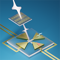 | K Peng, D Jevtics, F Zhang, S Sterzl, DA Damry, MU Rothmann, B Guilhabert, MJ Strain, HH Tan, LM Herz, L Fu, MD Dawson, A Hurtado, C Jagadish, MB Johnston
Science, 368:510--513 (May 2020)
[
pdf ][ SI ][ ref ]
Terahertz (THz) radiation is an interesting region of the electromagnetic spectrum lying between microwaves and infrared. Non-ionizing and transparent to most fabrics, it is finding application in security screening and imaging but is also being developed for communication and chemical sensing. To date, most THz detectors have focused just on signal intensity, an effort that discards half the signal in terms of the full optical state, including polarization. Peng et al. developed a THz detector based on crossed nanowires (arranged in a hash structure) that is capable of resolving the full state of the THz light. The approach provides a nanophotonic platform for the further development of THz-based technologies.Science, this issue p. 510Terahertz radiation encompasses a wide band of the electromagnetic spectrum, spanning from microwaves to infrared light, and is a particularly powerful tool for both fundamental scientific research and applications such as security screening, communications, quality control, and medical imaging. Considerable information can be conveyed by the full polarization state of terahertz light, yet to date, most time-domain terahertz detectors are sensitive to just one polarization component. Here we demonstrate a nanotechnology-based semiconductor detector using cross-nanowire networks that records the full polarization state of terahertz pulses. The monolithic device allows simultaneous measurements of the orthogonal components of the terahertz electric field vector without cross-talk. Furthermore, we demonstrate the capabilities of the detector for the study of metamaterials.
Citations: 110 (Scopus) 100 (Web of Science) |
- Trap states, electric fields, and phase segregation in mixed-halide perovskite photovoltaic devices
-
 | AJ Knight, JB Patel, HJ Snaith, MB Johnston, LM Herz
Adv. Energy Mater., 10:1903488 (Mar 2020)
[
pdf ][ SI ][ ref ]
Mixed-halide perovskites are essential for use in all-perovskite or perovskite-silicon tandem solar cells due to their tunable bandgap. However, trap states and halide segregation currently present the two main challenges for efficient mixed-halide perovskite technologies. Here photoluminescence techniques are used to study trap states and halide segregation in full mixed-halide perovskite photovoltaic devices. This work identifies three distinct defect species in the perovskite material: a charged, mobile defect that traps charge-carriers in the perovskite, a charge-neutral defect that induces halide segregation, and a charged, mobile defect that screens the perovskite from external electric fields. These three defects are proposed to be MA(+) interstitials, crystal distortions, and halide vacancies and/or interstitials, respectively. Finally, external quantum efficiency measurements show that photoexcited charge-carriers can be extracted from the iodide-rich low-bandgap regions of the phase-segregated perovskite formed under illumination, suggesting the existence of charge-carrier percolation pathways through grain boundaries where phase-segregation may occur.
Citations: 110 (Scopus) 110 (Web of Science) |
- Light absorption and recycling in hybrid metal halide perovskite photovoltaic devices
-
 | JB Patel, AD Wright, KB Lohmann, K Peng, CQ Xia, JM Ball, NK Noel, TW Crothers, J Wong-leung, HJ Snaith, LM Herz, MB Johnston
Adv. Energy Mater., 10:1903653 (Mar 2020)
[
pdf ][ SI ][ ref ]
The production of highly efficient single- and multijunction metal halide perovskite (MHP) solar cells requires careful optimization of the optical and electrical properties of these devices. Here, precise control of CH3NH3PbI3 perovskite layers is demonstrated in solar cell devices through the use of dual source coevaporation. Light absorption and device performance are tracked for incorporated MHP films ranging from approximate to 67 nm to approximate to 1.4 mu m thickness and transfer-matrix optical modeling is utilized to quantify optical losses that arise from interference effects. Based on these results, a device with 19.2% steady-state power conversion efficiency is achieved through incorporation of a perovskite film with near-optimum predicted thickness (approximate to 709 nm). Significantly, a clear signature of photon reabsorption is observed in perovskite films that have the same thickness (approximate to 709 nm) as in the optimized device. Despite the positive effect of photon recycling associated with photon reabsorption, devices with thicker (>750 nm) MHP layers exhibit poor performance owing to competing nonradiative charge recombination in a \"dead-volume\" of MHP. Overall, these findings demonstrate the need for fine control over MHP thickness to achieve the highest efficiency cells, and accurate consideration of photon reabsorption, optical interference, and charge transport properties.
Citations: 53 (Scopus) 50 (Web of Science) |
- Control over Crystal Size in Vapor Deposited Metal-Halide Perovskite Films
-
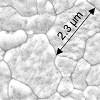 | KB Lohmann, JB Patel, MU Rothmann, CQ Xia, RDJ Oliver, LM Herz, HJ Snaith, MB Johnston
ACS Energy Lett., 5:710-717 (Mar 2020)
[
pdf ][ SI ][ ref ]
Understanding and controlling grain growth in metal halide perovskite polycrystalline thin films is an important step in improving the performance of perovskite solar cells. We demonstrate accurate control of crystallite size in CH3NH3PbI3 thin films by regulating substrate temperature during vacuum co-deposition of inorganic (PbI2) and organic (CH3NH3I) precursors. Films co-deposited onto a cold (−2 °C) substrate exhibited large, micrometer-sized crystal grains, while films that formed at room temperature (23 °C) only produced grains of 100 nm extent. We isolated the effects of substrate temperature on crystal growth by developing a new method to control sublimation of the organic precursor, and CH3NH3PbI3 solar cells deposited in this way yielded a power conversion efficiency of up to 18.2%. Furthermore, we found substrate temperature directly affects the adsorption rate of CH3NH3I, thus impacting crystal formation and hence solar cell device performance via changes to the conversion rate of PbI2 to CH3NH3PbI3 and stoichiometry. These findings offer new routes to developing efficient solar cells through reproducible control of crystal morphology and composition.
Citations: 103 (Scopus) 101 (Web of Science) |
- Dual-source coevaporation of low-bandgap $FA_{1-x}Cs_xSn_{1-y}Pb_yI_3$ perovskites for photovoltaics
-
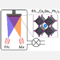 | JM Ball, L Buizza, HC Sansom, MD Farrar, MT Klug, J Borchert, J Patel, LM Herz, MB Johnston, HJ Snaith
ACS Energy Lett., 4:2748-2756 (Nov 2019)
[
pdf ][ SI ][ ref ]
Perovskite halides are well-suited to monolithic multijunction photovoltaics, promising low-cost solar-to-electrical power conversion. Critical to all-perovskite multijunction fabrication is the deposition of a low-bandgap absorber without damaging other device layers. Vapor deposition is thus an attractive method, obviating the need for optically lossy protective interlayers, but is challenging for multicomponent perovskites. Here, we demonstrate a method to dual-source coevaporate low-bandgap perovskite films and devices. We used mixtures formed by melting of metal halides as a single-crucible source of Cs, Pb, and Sn cations. Surprisingly, when this melt was coevaporated with formamidinium iodide (FM), uniform and dense perovskite films in the family( )FA(1-x)Cs(x)Sn(1-y)Pb(y)I(3 )were formed. Inclusion of SnF2 in the melt helped to regulate the perovskite\'s optoelectronic quality, leading to a steady-state power conversion efficiency of similar to 10% in a solar cell. This represents a new processing paradigm for evaporated perovskite alloys, which is an important step toward all-perovskite multijunction photovoltaics.
Citations: 62 (Scopus) 59 (Web of Science) |
- Charge-carrier dynamics, mobilities, and diffusion lengths of 2d-3d hybrid butylammonium-cesium-formamidinium lead halide perovskites
-
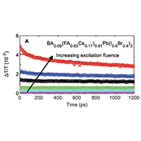 | LRV Buizza, TW Crothers, ZP Wang, JB Patel, RL Milot, HJ Snaith, MB Johnston, LM Herz
Adv. Funct. Mater., 29:1902656 (Aug 2019)
[
pdf ][ SI ][ ref ]
Perovskite solar cells (PSCs) have improved dramatically over the past decade, increasing in efficiency and gradually overcoming hurdles of temperature- and humidity-induced instability. Materials that combine high charge-carrier lifetimes and mobilities, strong absorption, and good crystallinity of 3D perovskites with the hydrophobic properties of 2D perovskites have become particularly promising candidates for use in solar cells. In order to fully understand the optoelectronic properties of these 2D-3D hybrid systems, the hybrid perovskite BA(x)(FA(0.83)Cs(0.17))(1-x)Pb(I0.6Br0.4)(3) is investigated across the composition range 0 <= x <= 0.8. Small amounts of butylammonium (BA) are found that help to improve crystallinity and appear to passivate grain boundaries, thus reducing trap-mediated charge-carrier recombination and enhancing charge-carrier mobilities. Excessive amounts of BA lead to poor crystallinity and inhomogeneous film formation, greatly reducing effective charge-carrier mobility. For low amounts of BA, the benevolent effects of reduced recombination and enhanced mobilities lead to charge-carrier diffusion lengths up to 7.7 mu m for x = 0.167. These measurements pave the way for highly efficient, highly stable PSCs and other optoelectronic devices based on 2D-3D hybrid materials.
Citations: 55 (Scopus) 53 (Web of Science) |
- Growth modes and quantum confinement in ultrathin vapour-deposited mapbi3 films
-
 | ES Parrott, JB Patel, AA Haghighirad, HJ Snaith, MB Johnston, LM Herz
Nanoscale, 11:14276-14284 (Aug 2019)
[
pdf ][ SI ][ ref ]
Vapour deposition of metal halide perovskite by co-evaporation of precursors has the potential to achieve large-area high-efficiency solar cells on an industrial scale, yet little is known about the growth of metal halide perovskites by this method at the current time. Here, we report the fabrication of MAPbI(3) films with average thicknesses from 2-320 nm by co-evaporation. We analyze the film properties using X-ray diffraction, optical absorption and photoluminescence (PL) to provide insights into the nucleation and growth of MAPbI(3) films on quartz substrates. We find that the perovskite initially forms crystallite islands of around 8 nm in height, which may be the cause of the persistent small grain sizes reported for evaporated metal halide perovskites that hinder device efficiency and stability. As more material is added, islands coalesce until full coverage of the substrate is reached at around 10 nm average thickness. We also find that quantum confinement induces substantial shifts to the PL wavelength when the average thickness is below 40 nm, offering dual-source vapour deposition as an alternative method of fabricating nanoscale structures for LEDs and other devices.
Citations: 80 (Scopus) 77 (Web of Science) |
- Impurity Tracking Enables Enhanced Control and Reproducibility of Hybrid Perovskite Vapor Deposition
-
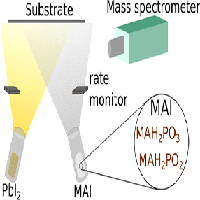 | J Borchert, I Levchuk, LC Snoek, MU Rothmann, R Haver, HJ Snaith, CJ Brabec, LM Herz, MB Johnston
ACS Appl. Mater. Interfaces, 11:28851-28857 (Jul 2019)
[
pdf ][ SI ][ ref ]
Metal halide perovskite semiconductors have the potential to enable low-cost, flexible, and efficient solar cells for a wide range of applications. Physical vapor deposition by co-evaporation of precursors is a method that results in very smooth and pinhole-free perovskite thin films and allows excellent control over film thickness and composition. However, for a deposition method to become industrially scalable, reproducible process control and high device yields are essential. Unfortunately, to date, the control and reproducibility of evaporating organic precursors such as methylammonium iodide (MAI) have proved extremely challenging. We show that the established method of controlling the evaporation rate of MAI with quartz microbalances (QMBs) is critically sensitive to the concentration of the impurities MAH2PO3 and MAH2PO2 that are usually present in MAI after synthesis. Therefore, controlling the deposition rate of MAI with QMBs is unreliable since the concentration of such impurities typically varies from one batch of MAI to another and even during the course of a deposition. However once reliable control of MAI deposition is achieved, we find that the presence of precursor impurities during perovskite deposition does not degrade the solar cell performance. Our results indicate that as long as precursor deposition rates are well controlled, physical vapor deposition will allow high solar cell device yields even if the purity of precursors changes from one run to another.
Citations: 63 (Scopus) 58 (Web of Science) |
- Heterogeneous photon recycling and charge diffusion enhance charge transport in quasi-2d lead-halide perovskite films
-
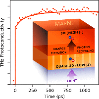 | SG Motti, T Crothers, R Yang, Y Cao, RZ Li, MB Johnston, JP Wang, LM Herz
Nano Lett., 19:3953-3960 (Jun 2019)
[
pdf ][ SI ][ ref ]
The addition of large hydrophobic cations to lead halide perovskites has significantly enhanced the environmental stability of photovoltaic cells based on these materials. However, the associated formation of two-dimensional structures inside the material can lead to dielectric confinement, higher exciton binding energies, wider bandgaps and limited charge-carrier mobilities. Here we show that such effects are not detrimental to the charge transport for carefully processed films comprising a self-assembled thin layer of quasi-two-dimensional (2D) perovskite interfaced with a 3D MAPbI(3) perovskite layer. We apply a combination of time-resolved photoluminescence and photoconductivity spectroscopy to reveal the charge-carrier recombination and transport through the film profile, when either the quasi-2D or the 3D layers are selectively excited. Through modeling of the recorded dynamics, we demonstrate that while the charge-carrier mobility is lower within the quasi-2D region, charge-carrier diffusion to the 3D phase leads to a rapid recovery in photoconductivity even when the quasi-2D region is initially photoexcited. In addition, the blue-shifted emission originating from quasi-2D regions overlaps significantly with the absorption spectrum of the 3D perovskite, allowing for highly effective \"heterogeneous photon recycling\". We show that this combination fully compensates for the adverse effects of electronic confinement, yielding quasi-2D perovskites with highly efficient charge transporting properties.
Citations: 77 (Scopus) 73 (Web of Science) |
- Effect of ultraviolet radiation on organic photovoltaic materials and devices
-
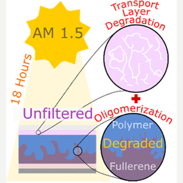 | JB Patel, P Tiwana, N Seidler, GE Morse, OR Lozman, MB Johnston, LM Herz
ACS Appl. Mater. Interfaces, 11:21543-21551 (Jun 2019)
[
pdf ][ SI ][ ref ]
Organic photovoltaics are a sustainable and cost-effective power-generation technology that may aid the move to zero-emission buildings, carbon neutral cities, and electric vehicles. While state-of-the-art organic photovoltaic devices can be encapsulated to withstand air and moisture, they are currently still susceptible to light-induced degradation, leading to a decline in the long-term efficiency of the devices. In this study, the role of ultraviolet (UV) radiation on a multilayer ,organic photovoltaic device is systematically uncovered using spectral filtering. By applying long-pass filters to remove different parts of the UV portion of the AM1.5G spectrum, two main photodegradation processes are shown to occur in the organic photovoltaic devices. A UV-activated process is found to cause a significant decrease in the photocurrent across the whole spectrum and is most likely linked to the deterioration of the charge extraction layers. In addition, a photodegradation process caused by UV-filtered sunlight is found to change the micromorphology of the bulk heterojunction material, leading to a reduction in photocurrent at high photon energies. These findings strongly suggest that the fabrication of inherently photostable organic photovoltaic devices will require the replacement of fullerene-based electron transporter materials with alternative organic semiconductors.
Citations: 54 (Scopus) 51 (Web of Science) |
- Solution-processed all-perovskite multi-junction solar cells
-
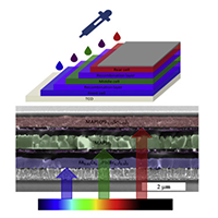 | DP McMeekin, S Mahesh, NK Noel, MT Klug, J Lim, JH Warby, JM Ball, LM Herz, MB Johnston, HJ Snaith
Joule, 3:387-401 (Feb 2019)
[
pdf ][ SI ][ ref ]
Multi-junction device architectures can increase the power conversion efficiency (PCE) of photovoltaic (PV) cells beyond the single-junction thermodynamic limit. However, these devices are challenging to produce by solution-based methods, where dissolution of underlying layers is problematic. By employing a highly volatile acetonitrile(CH3CN)/methylamine(CH3NH2) (ACN/MA) solvent-based perovskite solution, we demonstrate fully solution-processed absorber, transport, and recombination layers for monolithic all-perovskite tandem and triple-junction solar cells. By combining FA(0.83)Cs(0.17)Pb(Br0.7I0.3)(3) (1.94 eV) and MAPbI(3) (1.57 eV) junctions, we reach two-terminal tandem PCEs of more than 15% (steady state). We show that a MAPb(0.75)Sn(0.25)I(3) (1.34 eV) narrow band-gap perovskite can be processed via the ACN/MA solvent-based system, demonstrating the first proof-of-concept, monolithic all-perovskite triple-junction solar cell with an open-circuit voltage reaching 2.83 V. Through optical and electronic modeling, we estimate the achievable PCE of a state-of-the-art triple-junction device architecture to be 26.7%. Our work opens new possibilities for large-scale, low-cost, printable perovskite multi-junction solar cells.
Citations: 222 (Scopus) 211 (Web of Science) |
- Elucidating the long-range charge carrier mobility in metal halide perovskite thin films
-
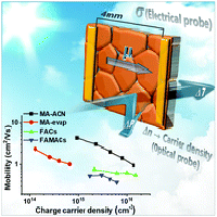 | J Lim, MT Horantner, N Sakai, JM Ball, S Mahesh, NK Noel, YH Lin, JB Patel, DP McMeekin, MB Johnston, B Wenger, HJ Snaith
Energy Environ. Sci., 12:169-176 (Jan 2019)
[
pdf ][ SI ][ ref ]
Many optoelectronic properties have been reported for lead halide perovskite polycrystalline films. However, ambiguities in the evaluation of these properties remain, especially for long-range lateral charge transport, where ionic conduction can complicate interpretation of data. Here we demonstrate a new technique to measure the long-range charge carrier mobility in such materials. We combine quasi-steady-state photo-conductivity measurements (electrical probe) with photo-induced transmission and reflection measurements (optical probe) to simultaneously evaluate the conductivity and charge carrier density. With this knowledge we determine the lateral mobility to be approximate to 2 cm(2) V-1 s(-1) for CH3NH3PbI3 (MAPbI(3)) polycrystalline perovskite films prepared from the acetonitrile/methylamine solvent system. Furthermore, we present significant differences in long-range charge carrier mobilities, from 2.2 to 0.2 cm(2) V-1 s(-1), between films of contemporary perovskite compositions prepared via different fabrication processes, including solution and vapour phase deposition techniques. Arguably, our work provides the first accurate evaluation of the long-range lateral charge carrier mobility in lead halide perovskite films, with charge carrier density in the range typically achieved under photovoltaic operation.
Citations: 175 (Scopus) 171 (Web of Science) |
- Electronic traps and phase segregation in lead mixed-halide perovskite
-
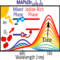 | AJ Knight, AD Wright, JB Patel, DP McMeekin, HJ Snaith, MB Johnston, LM Herz
ACS Energy Lett., 4:75-84 (Jan 2019)
[
pdf ][ SI ][ ref ]
An understanding of the factors driving halide segregation in lead mixed-halide perovskites is required for their implementation in tandem solar cells with existing silicon technology. Here we report that the halide segregation dynamics observed in the photoluminescence from CH3NH3Pb(Br0.5I0.5)(3) is strongly influenced by the atmospheric environment, and that encapsulation of films with a layer of poly(methyl methacrylate) allows for halide segregation dynamics to be fully reversible and repeatable. We further establish an empirical model directly linking the amount of halide segregation observed in the photoluminescence to the fraction of charge carriers recombining through trap-mediated channels, and the photon flux absorbed. From such quantitative analysis we show that under pulsed illumination, the frequency of the modulation alone has no influence on the segregation dynamics. Additionally, we extrapolate that working CH3NH3Pb(Br0.5I0.5)(3) perovskite cells would require a reduction of the trap-related charge carrier recombination rate to less than or similar to 10(5)s(-1) in order for halide segregation to be sufficiently suppressed.
Citations: 272 (Scopus) 269 (Web of Science) |
- Temperature-dependent refractive index of quartz at terahertz frequencies
-
 | CL Davies, JB Patel, CQ Xia, LM Herz, MB Johnston
J. Infrared Millim. Terahertz Waves, 39:1236-1248 (Dec 2018)
[
pdf ][ SI ][ ref ]
Characterisation of materials often requires the use of a substrate to support the sample being investigated. For optical characterisation at terahertz frequencies, quartz is commonly used owing to its high transmission and low absorption at these frequencies. Knowledge of the complex refractive index of quartz is required for analysis of time-domain terahertz spectroscopy and optical pump terahertz probe spectroscopy for samples on a quartz substrate. Here, we present the refractive index and extinction coefficient for alpha-quartz between 0.5 THz and 5.5 THz (17-183 cm(-1)) taken at 10, 40, 80, 120, 160, 200 and 300 K. Quartz shows excellent transmission and is thus an ideal optical substrate over the THz band, apart from the region 3.9 +/- 0.1 THz owing to a spectral feature originating from the lowest energy optical phonon modes. We also present the experimentally measured polariton dispersion of alpha-quartz over this frequency range.
Citations: 94 (Scopus) 90 (Web of Science) |
- The effects of doping density and temperature on the optoelectronic properties of formamidinium tin triiodide thin films
-
 | RL Milot, MT Klug, CL Davies, Z Wang, H Kraus, HJ Snaith, MB Johnston, LM Herz
Adv. Mater., 30:1804506 (Nov 2018)
[
pdf ][ SI ][ ref ]
Optoelectronic properties are unraveled for formamidinium tin triiodide (FASnI(3)) thin films, whose background hole doping density is varied through SnF2 addition during film fabrication. Monomolecular charge-carrier recombination exhibits both a dopant-mediated part that grows linearly with hole doping density and remnant contributions that remain under tin-enriched processing conditions. At hole densities near 10(20) cm(-3), a strong Burstein-Moss effect increases absorption onset energies by approximate to 300 meV beyond the bandgap energy of undoped FASnI(3) (shown to be 1.2 eV at 5 K and 1.35 eV at room temperature). At very high doping densities (10(20) cm(-3)), temperature-dependent measurements indicate that the effective charge-carrier mobility is suppressed through scattering with ionized dopants. Once the background hole concentration is nearer 10(19) cm(-3) and below, the charge-carrier mobility increases with decreasing temperature according to approximate to T-1.2, suggesting that it is limited mostly by intrinsic interactions with lattice vibrations. For the lowest doping concentration of 7.2 x 10(18) cm(-3), charge-carrier mobilities reach a value of 67 cm(2) V-1 s(-1) at room temperature and 470 cm(2) V-1 s(-1) at 50 K. Intraexcitonic transitions observed in the THz-frequency photoconductivity spectra at 5 K reveal an exciton binding energy of only 3.1 meV for FASnI(3), in agreement with the low bandgap energy exhibited by this perovskite.
Citations: 211 (Scopus) 209 (Web of Science) |
- High irradiance performance of metal halide perovskites for concentrator photovoltaics
-
 | ZP Wang, QQ Lin, B Wenger, MG Christoforo, YH Lin, MT Klug, MB Johnston, LM Herz, HJ Snaith
Nat. Energy, 3:855-861 (Oct 2018)
[
pdf ][ SI ][ ref ]
Traditionally, III-V multi-junction cells have been used in concentrator photovoltaic (CPV) applications, which deliver extremely high efficiencies but have failed to compete with \'flat-plate\' silicon technologies owing to cost. Here, we assess the feasibility of using metal halide perovskites for CPVs, and we evaluate their device performance and stability under concentrated light. Under simulated sunlight, we achieve a peak efficiency of 23.6% under 14 Suns (that is,14 times the standard solar irradiance), as compared to 21.1% under 1 Sun, and measure 1.26 V open-circuit voltage under 53 Suns, for a material with a bandgap of 1.63 eV. Importantly, our encapsulated devices maintain over 90% of their original efficiency after 150 h aging under 10 Suns at maximum power point. Our work reveals the potential of perovskite CPVs, and may lead to new PV deployment strategies combining perovskites with low-concentration factor and lower-accuracy solar tracking systems.
Citations: 213 (Scopus) 203 (Web of Science) |
- Raman spectrum of the organic-inorganic halide perovskite ch3nh3pbi3 from first principles and high-resolution low-temperature raman measurements
-
 | MA Perez-Osorio, QQ Lin, RT Phillips, RL Milot, LM Herz, MB Johnston, F Giustino
J. Phys. Chem. C, 122:21703-21717 (Sep 2018)
[
pdf ][ SI ][ ref ]
We investigate the Raman spectrum of the low temperature orthorhombic phase of the organic-inorganic halide perovskite CH3NH3PbI3, by combining first-principles calculations with high-resolution low-temperature Raman measurements. We find good agreement between theory and experiment and successfully assign each of the Raman peaks to the underlying vibrational modes. In the low frequency spectral range (below 60 cm(-1)), we assign the prominent Raman signals at 26, 32, 42, and 49 cm(-1) to the Pb-I-Pb bending modes with either A(g) or B-2g symmetry and the signal at 58 cm(-1) to the librational mode of the organic cation. Owing to their significant intensity, we propose that these peaks can serve as clear markers of the vibrations of the [PbI3](-) network and of the CH3NH3+ cations in this perovskite, respectively. In particular, the ratios of the intensities of these peaks might be used to monitor possible deviations from the ideal stoichiometry of CH3NH3PbI3.
Citations: 116 (Scopus) 113 (Web of Science) |
- Impact of the organic cation on the optoelectronic properties of formamidinium lead triiodide
-
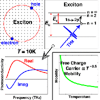 | CL Davies, J Borchert, CQ Xia, RL Milot, H Kraus, MB Johnston, LM Herz
J. Phys. Chem. Lett., 9:4502-4511 (Aug 2018)
[
pdf ][ SI ][ ref ]
Metal halide perovskites have proven to be excellent light-harvesting materials in photovoltaic devices whose efficiencies are rapidly improving. Here, we examine the temperature-dependent photon absorption, exciton binding energy, and band gap of FAPbI(3) (thin film) and find remarkably different behavior across the beta-gamma phase transition compared with MAPbI(3). While MAPbI(3) has shown abrupt changes in the band gap and exciton binding energy, values for FAPbI(3) vary smoothly over a range of 100-160 K in accordance with a more gradual transition. In addition, we find that the charge-carrier mobility in FAPbI(3) exhibits a clear T-0.5 trend with temperature, in excellent agreement with theoretical predictions that assume electron-phonon interactions to be governed by the Frohlich mechanism but in contrast to the T-0.5 dependence previously observed for MAPbI(3). Finally, we directly observe intraexcitonic transitions in FAPbI(3) at low temperature, from which we determine a low exciton binding energy of only 5.3 meV at 10 K.
Citations: 59 (Scopus) 57 (Web of Science) |
- Interplay of structural and optoelectronic properties in formamidinium mixed tin-lead triiodide perovskites
-
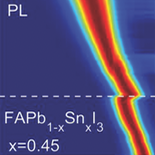 | ES Parrott, T Green, RL Milot, MB Johnston, HJ Snaith, LM Herz
Adv. Funct. Mater., 28:1802803 (Aug 2018)
[
pdf ][ SI ][ ref ]
Mixed lead-tin triiodide perovskites are promising absorber materials for low bandgap bottom cells in all-perovskite tandem photovoltaic devices. Key structural and electronic properties of the FAPb(1-x)Sn(x)I(3) perovskite are presented here as a function of lead: tin content across the alloy series. Temperature-dependent photoluminescence and optical absorption measurements are used to identify changes in the bandgap and phase transition temperature. The large bandgap bowing parameter, a crucial element for the attainment of low bandgaps in this system, is shown to depend on the structural phase, reaching a value of 0.84 eV in the low-temperature phase and 0.73 eV at room temperature. The parabolic nature of the bowing at all temperatures is compatible with a mechanism arising from bond bending to accommodate the random placement of unevenly sized lead and tin ions. Charge-carrier recombination dynamics are shown to fall into two regimes. Tin-rich compositions exhibit fast, monoexponential recombination that is almost temperature-independent, in accordance with high levels of electrical doping. Lead-rich compositions show slower, stretched-exponential charge-carrier recombination that is strongly temperature-dependent, in accordance with a multiphonon assisted process. These results highlight the importance of structure and composition for control of bandgap bowing and charge-carrier recombination mechanisms in low bandgap absorbers for all-perovskite tandem solar cells.
Citations: 72 (Scopus) 71 (Web of Science) |
- Highly crystalline methylammonium lead tribromide perovskite films for efficient photovoltaic devices
-
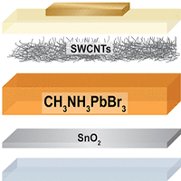 | NK Noel, B Wenger, SN Habisreutinger, JB Patel, T Crothers, ZP Wang, RJ Nicholas, MB Johnston, LM Herz, HJ Snaith
ACS Energy Lett., 3:1233-1240 (Jun 2018)
[
pdf ][ SI ][ ref ]
The rise of metal-halide perovskite solar cells has captivated the research community, promising to disrupt the current energy landscape. While a sizable percentage of the research done on this class of materials has been focused on the neat and iodide-rich perovskites, bromide-based perovskites can deliver substantially higher voltages because of their relatively wide band gaps of over 2 eV. The potential for efficient, high-voltage devices makes materials such as these incredibly attractive for multijunction photovoltaic applications. Here, we use the acetonitrile/methylamine solvent system to deposit smooth, highly crystalline films of CH3NH3PbBr3. By using choline chloride as a passivating agent for these films, we achieve photoluminescence quantum efficiencies of up to 5.5% and demonstrate charge-carrier mobilities of 17.8 cm(2)/(V s). Incorporating these films into photovoltaic devices, we achieve scanned power conversion efficiencies of up to 8.9%, with stabilized efficiencies of 7.6%, providing a simple route to realizing efficient, high-voltage CH3NH3PbBr3 planar-heterojunction devices.
Citations: 59 (Scopus) 59 (Web of Science) |
- High electron mobility and insights into temperature-dependent scattering mechanisms in inassb nanowires
-
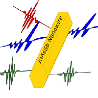 | JL Boland, F Amaduzzi, S Sterzl, H Potts, LM Herz, AFI Morral, MB Johnston
Nano Lett., 18:3703-3710 (Jun 2018)
[
pdf ][ SI ][ ref ]
InAsSb nanowires are promising elements for thermoelectric devices, infrared photodetectors, high-speed transistors, as well as thermophotovoltaic cells. By changing the Sb alloy fraction the mid-infrared bandgap energy and thermal conductivity may be tuned for specific device applications. Using both terahertz and Raman noncontact probes, we show that Sb alloying increases the electron mobility in the nanowires by over a factor of 3 from InAs to InAs0.65Sb0.35. We also extract the temperature-dependent electron mobility via both terahertz and Raman spectroscopy, and we report the highest electron mobilities for InAs0.65Sb0.35 nanowires to date, exceeding 16,000 cm(2) V-1 s(-1) at 10 K.
Citations: 36 (Scopus) 35 (Web of Science) |
- Hybrid perovskites: prospects for concentrator solar cells
-
 | QQ Lin, ZP Wang, HJ Snaith, MB Johnston, LM Herz
Adv. Sci., 5:1700792 (Apr 2018)
[
pdf ][ SI ][ ref ]
Perovskite solar cells have shown a meteoric rise of power conversion efficiency and a steady pace of improvements in their stability of operation. Such rapid progress has triggered research into approaches that can boost efficiencies beyond the Shockley-Queisser limit stipulated for a single-junction cell under normal solar illumination conditions. The tandem solar cell architecture is one concept here that has recently been successfully implemented. However, the approach of solar concentration has not been sufficiently explored so far for perovskite photovoltaics, despite its frequent use in the area of inorganic semiconductor solar cells. Here, the prospects of hybrid perovskites are assessed for use in concentrator solar cells. Solar cell performance parameters are theoretically predicted as a function of solar concentration levels, based on representative assumptions of charge-carrier recombination and extraction rates in the device. It is demonstrated that perovskite solar cells can fundamentally exhibit appreciably higher energy-conversion efficiencies under solar concentration, where they are able to exceed the Shockley-Queisser limit and exhibit strongly elevated open-circuit voltages. It is therefore concluded that sufficient material and device stability under increased illumination levels will be the only significant challenge to perovskite concentrator solar cell applications.
Citations: 89 (Scopus) 83 (Web of Science) |
- Bimolecular recombination in methylammonium lead triiodide perovskite is an inverse absorption process
-
 | CL Davies, MR Filip, JB Patel, TW Crothers, C Verdi, AD Wright, RL Milot, F Giustino, MB Johnston, LM Herz
Nat. Commun., 9:293 (Jan 2018)
[
pdf ][ SI ][ ref ]
Photovoltaic devices based on metal halide perovskites are rapidly improving in efficiency. Once the Shockley-Queisser limit is reached, charge-carrier extraction will be limited only by radiative bimolecular recombination of electrons with holes. Yet, this fundamental process, and its link with material stoichiometry, is still poorly understood. Here we show that bimolecular charge-carrier recombination in methylammonium lead triiodide perovskite can be fully explained as the inverse process of absorption. By correctly accounting for contributions to the absorption from excitons and electron-hole continuum states, we are able to utilise the van Roosbroeck-Shockley relation to determine bimolecular recombination rate constants from absorption spectra. We show that the sharpening of photon, electron and hole distribution functions significantly enhances bimolecular charge recombination as the temperature is lowered, mirroring trends in transient spectroscopy. Our findings provide vital understanding of band-to-band recombination processes in this hybrid perovskite, which comprise direct, fully radiative transitions between thermalized electrons and holes.
Citations: 307 (Scopus) 308 (Web of Science) |
- Photocurrent spectroscopy of perovskite solar cells over a wide temperature range from 15 to 350 k
-
 | JB Patel, QQ Lin, O Zadvorna, CL Davies, LM Herz, MB Johnston
J. Phys. Chem. Lett., 9:263-268 (Jan 2018)
[
pdf ][ SI ][ ref ]
Solar cells based on metal halide perovskite thin films show great promise for energy generation in a range of environments from terrestrial installations to space applications. Here we assess the device characteristics of the prototypical perovskite solar cells based on methylammonium lead triiodide (CH3NH3PbI3) over a broad temperature range from 15 to 350 K (-258 to 77 degrees C). For these devices, we observe a peak in the short-circuit current density and open-circuit voltage at 200 K (-73 degrees C) with decent operation maintained up to 350 K. We identify the clear signature of crystalline PbI2 contributing directly to the low-temperature photocurrent spectra, showing that PbI2 plays an active role (beyond passivation) in CH3NH3PbI3 solar cells. Finally we observe a blue-shift in the photocurrent spectrum with respect to the absorption spectrum at low temperature (15 K), allowing us to extract a lower limit on the exciton binding energy of 9.1 meV for CH3NH3PbI3.
Citations: 25 (Scopus) 25 (Web of Science) |
- Modification of the fluorinated tin oxide/electron-transporting material interface by a strong reductant and its effect on perovskite solar cell efficiency
-
 | F Pulvirenti, B Wegner, NK Noel, G Mazzotta, R Hill, JB Patel, LM Herz, MB Johnston, MK Riede, HJ Snaith, N Koch, S Barlow, SR Marder
Mol. Syst. Des. Eng., 3:741-747 ( 2018)
[
pdf ][ SI ][ ref ]
To date, the most efficient hybrid metal halide peroskite solar cells employ TiO2 as electron-transporting material (ETM), making these devices unstable under UV light exposure. Replacing TiO2 with fullerene derivatives has been shown to result in improved electronic contact and increased device lifetime, making it of interest to assess whether similar improvements can be achieved by using other organic semiconductors as ETMs. In this work, we investigate perylene-3,4:9,10-tetracarboxylic bis(benzimidazole) as a vacuum-processable ETM, and we minimize electron-collection losses at the electron-selective contact by depositing pentamethylcyclopentadienyl cyclopentadienyl rhodium dimer, (RhCp*Cp)(2), on fluorinated tin oxide. With (RhCp*Cp)(2) as an interlayer, ohmic contacts can be formed, there is interfacial doping of the ETM, and stabilized power conversion efficiencies of up to 14.2% are obtained.
|
- Large-Area, Highly Uniform Evaporated Formamidinium Lead Triiodide Thin Films for Solar Cells
-
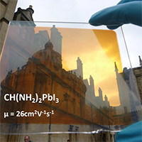 | J Borchert, RL Milot, JB Patel, CL Davies, AD Wright, L Martinez Maestro, HJ Snaith, LM Herz, MB Johnston
ACS Energy Lett., 2:2799-2804 (Nov 2017)
[
pdf ][ SI ][ ref ]
Perovskite thin-film solar cells are one of the most promising emerging renewable energy technologies because of their potential for low-cost, large-area fabrication combined with high energy conversion efficiencies. Recently, formamidinium lead triiodide ($\rm {FAPbI_3}$) and other formamidinium (CH(NH$_2$)$_2$) based perovskites have been explored as interesting alternatives to methylammonium lead triiodide ($\rm {MAPbI_3}$), because they exhibit better thermal stability. However at present a major challenge is up-scaling of perovskite solar cells from small test-cells to full solar modules. We show that co-evaporation is a scalable method for the deposition of homogeneous $\rm FAPbI_3$ thin-films over large areas. The method allows precise control over film thickness and results in highly uniform, pin-hole free layers. Our films exhibited a high charge-carrier mobility of 26\,$\rm cm^2 V^{-1}s^{-1}$, excellent optical properties and a bimolecular recombination constant of $7\times10^{-11}$\,cm$^3$s$^{-1}$. Solar cells fabricated using these vapor-deposited layers within a regular device architecture produced stabilized power conversion efficiencies of up to 14.2\,$\rm\%$. Thus we demonstrate that efficient $\rm FAPbI_3$ solar cells can be vapor-deposited, which opens up a pathway towards large-area stable perovskite photovoltaics.
Citations: 145 (Scopus) 137 (Web of Science) |
- Near-infrared and short-wavelength infrared photodiodes based on dye-perovskite composites
-
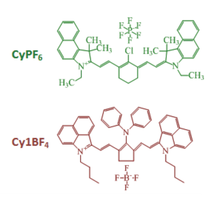 | QQ Lin, ZP Wang, M Young, JB Patel, RL Milot, LM Maestro, RR Lunt, HJ Snaith, MB Johnston, LM Herz
Adv. Funct. Mater., 27:1702485 (Oct 2017)
[
pdf ][ SI ][ ref ]
Organohalide perovskites have emerged as promising light-sensing materials because of their superior optoelectronic properties and low-cost processing methods. Recently, perovskite-based photodetectors have successfully been demonstrated as both broadband and narrowband varieties. However, the photodetection bandwidth in perovskite-based photodetectors has so far been limited to the near-infrared regime owing to the relatively wide band gap of hybrid organohalide perovskites. In particular, short-wavelength infrared photodiodes operating beyond 1 mu m have not yet been realized with organohalide perovskites. In this study, narrow band gap organic dyes are combined with hybrid perovskites to form composite films as active photoresponsive layers. Tuning the dye loading allows for optimization of the spectral response characteristics and excellent charge-carrier mobilities near 11 cm(2) V-1 s(-1), suggesting that these composites combine the light-absorbing properties or IR dyes with the outstanding charge-extraction characteristics of the perovskite. This study demonstrates the first perovskite photodiodes with deep near-infrared and short-wavelength infrared response that extends as far as 1.6 mu m. All devices are solution-processed and exhibit relatively high responsivity, low dark current, and fast response at room temperature, making this approach highly attractive for next-generation light-detection techniques.
Citations: 77 (Scopus) 73 (Web of Science) |
- Unveiling the influence of ph on the crystallization of hybrid perovskites, delivering low voltage loss photovoltaics
-
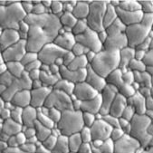 | NK Noel, M Congiu, AJ Ramadan, S Fearn, DP McMeekin, JB Patel, MB Johnston, B Wenger, HJ Snaith
Joule, 1:328-343 (Oct 2017)
[
pdf ][ SI ][ ref ]
Impressive power conversion efficiencies coupled with the relative ease of fabrication have made perovskite solar cells a front runner for next-generation photovoltaics. Although perovskite films and optoelectronic devices have been widely studied, relatively little is known about the chemistry of the precursor solutions. Here, we present a study on the hydrolysis of N, N-dimethylformamide, correlating how pH changes related to its degradation affect the crystallization of MAPbI(3-x)Cl(x) perovskite films. By careful manipulation of the pH, and the resulting colloid distribution in precursor solutions, we fabricate perovskite films with greatly improved crystallinity, which when incorporated into photovoltaic devices reproducibly yield efficiencies of over 18%. Extending this method to the mixed cation, mixed halide perovskite FA(0.83)MA(0.17)Pb(I0.83Br0.17)(3), we obtain power conversion efficiencies of up to 19.9% and open-circuit voltages of 1.21 V for a material with a bandgap of 1.57 eV, achieving the lowest yet reported loss in potential from bandgap to a V-OC of only 360 mV.
Citations: 181 (Scopus) 179 (Web of Science) |
- Photon reabsorption masks intrinsic bimolecular charge-carrier recombination in {CH$_3$NH$_3$PbI$_3$} perovskite
-
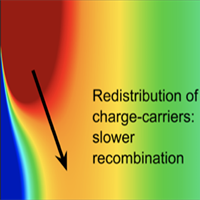 | TW Crothers, RL Milot, JB Patel, ES Parrott, J Schlipf, P Muller-buschbaum, MB Johnston, LM Herz
Nano Lett., 17:5782-5789 (Sep 2017)
[
pdf ][ SI ][ ref ]
An understanding of charge-carrier recombination processes is essential for the development of hybrid metal halide perovskites for photovoltaic applications. We show that typical measurements of the radiative bimolecular recombination constant in CH3NH3PbI3 are strongly affected by photon reabsorption that masks a much larger intrinsic bimolecular recombination rate constant. By investigating a set of films whose thickness varies between 50 and 533 nm, we find that the bimolecular charge recombination rate appears to slow by an order of magnitude as the film thickness increases. However, by using a dynamical model that accounts for photon reabsorption and charge-carrier diffusion we determine that a single intrinsic bimolecular recombination coefficient of value 6.8 X 10(-10) cm(3)s(-1) is common to all samples irrespective of film thickness. Hence, we postulate that the wide range of literature values reported for such coefficients is partly to blame on differences in photon out-coupling between samples with crystal grains or mesoporous scaffolds of different sizes influencing light scattering, whereas thinner films or index-matched surrounding layers can reduce the possibility for photon reabsorption. We discuss the critical role of photon confinement on free charge-carrier retention in thin photovoltaic layers and highlight an approach to assess the success of such schemes from transient spectroscopic measurement.
Citations: 161 (Scopus) 156 (Web of Science) |
- Crystallization kinetics and morphology control of formamidinium-cesium mixed-cation lead mixed-halide perovskite via tunability of the colloidal precursor solution
-
 | DP McMeekin, ZP Wang, W Rehman, F Pulvirenti, JB Patel, NK Noel, MB Johnston, SR Marder, LM Herz, HJ Snaith
Adv. Mater., 29:1607039 (Aug 2017)
[
pdf ][ SI ][ ref ]
The meteoric rise of the field of perovskite solar cells has been fueled by the ease with which a wide range of high-quality materials can be fabricated via simple solution processing methods. However, to date, little effort has been devoted to understanding the precursor solutions, and the role of additives such as hydrohalic acids upon film crystallization and final optoelectronic quality. Here, a direct link between the colloids concentration present in the [HC(NH2)(2)](0.83)Cs0.17Pb(Br0.2I0.8)(3) precursor solution and the nucleation and growth stages of the thin film formation is established. Using dynamic light scattering analysis, the dissolution of colloids over a time span triggered by the addition of hydrohalic acids is monitored. These colloids appear to provide nucleation sites for the perovskite crystallization, which critically impacts morphology, crystal quality, and optoelectronic properties. Via 2D X-ray diffraction, highly ordered and textured crystals for films prepared from solutions with lower colloidal concentrations are observed. This increase in material quality allows for a reduction in microstrain along with a twofold increase in charge-carrier mobilities leading to values exceeding 20 cm(2) V-1 s(-1). Using a solution with an optimized colloidal concentration, devices that reach current-voltage measured power conversion efficiency of 18.8% and stabilized efficiency of 17.9% are fabricated.
Citations: 310 (Scopus) 295 (Web of Science) |
- Band-tail recombination in hybrid lead iodide perovskite
-
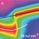 | AD Wright, RL Milot, GE Eperon, HJ Snaith, MB Johnston, LM Herz
Adv. Funct. Mater., 27:1700860 (Aug 2017)
[
pdf ][ SI ][ ref ]
Traps limit the photovoltaic efficiency and affect the charge transport of optoelectronic devices based on hybrid lead halide perovskites. Understanding the nature and energy scale of these trap states is therefore crucial for the development and optimization of solar cell and laser technology based on these materials. Here, the low-temperature photoluminescence of formamidinium lead triiodide (HC(NH2)(2)PbI3) is investigated. A power-law time dependence in the emission intensity and an additional low-energy emission peak that exhibits an anomalous relative Stokes shift are observed. Using a rate-equation model and a Monte Carlo simulation, it is revealed that both phenomena arise from an exponential trap-density tail with characteristic energy scale of approximate to 3 meV. Charge-carrier recombination from sites deep within the tail is found to cause emission with energy downshifted by up to several tens of meV. Hence, such phenomena may in part be responsible for open-circuit voltage losses commonly observed in these materials. In this high-quality hybrid perovskite, trap states thus predominantly comprise a continuum of energetic levels (associated with disorder) rather than discrete trap energy levels (associated, e.g., with elemental vacancies). Hybrid perovskites may therefore be viewed as classic semiconductors whose band-structure picture is moderated by a modest degree of energetic disorder.
Citations: 161 (Scopus) 152 (Web of Science) |
- Towards higher electron mobility in modulation doped {GaAs/AlGaAs} core shell nanowires
-
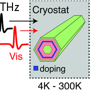 | JL Boland, G Tutuncuoglu, JQ Gong, S Conesa-boj, CL Davies, LM Herz, AFI Morral, MB Johnston
Nanoscale, 9:7839-7846 (Jun 2017)
[
pdf ][ SI ][ ref ]
Precise control over the electrical conductivity of semiconductor nanowires is a crucial prerequisite for implementation of these nanostructures into novel electronic and optoelectronic devices. Advances in our understanding of doping mechanisms in nanowires and their influence on electron mobility and radiative efficiency are urgently required. Here, we investigate the electronic properties of n-type modulation doped GaAs/AlGaAs nanowires via optical pump terahertz (THz) probe spectroscopy and photoluminescence spectroscopy over the temperature range 5 K-300 K. We directly determine an ionization energy of 6.7 +/- 0.5 meV (T = 52 K) for the Si donors within the AlGaAs shell that create the modulation doping structure. We further elucidate the temperature dependence of the electron mobility, photoconductivity lifetime and radiative efficiency, and determine the charge-carrier scattering mechanisms that limit electron mobility. We show that below the donor ionization temperature, charge scattering is limited by interactions with interfaces, leading to an excellent electron mobility of 4360 +/- 380 cm(2) V-1 s(-1) at 5 K. Above the ionization temperature, polar scattering via longitudinal optical (LO) phonons dominates, leading to a room temperature mobility of 2220 +/- 130 cm(2) V-1 s(-1). In addition, we show that the Si donors effectively passivate interfacial trap states in the nanowires, leading to prolonged photoconductivity lifetimes with increasing temperature, accompanied by an enhanced radiative efficiency that exceeds 10% at room temperature.
Citations: 18 (Scopus) 18 (Web of Science) |
- The influence of surfaces on the transient terahertz conductivity and electron mobility of {GaAs} nanowires
-
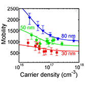 | HJ Joyce, SA Baig, P Parkinson, CL Davies, JL Boland, HH Tan, C Jagadish, LM Herz, MB Johnston
J. Phys. D-Appl. Phys., 50:224001 (Jun 2017)
[
pdf ][ SI ][ ref ]
Bare unpassivated GaAs nanowires feature relatively high electron mobilities (400-2100 cm(2) V-1 s(-1)) and ultrashort charge carrier lifetimes (1-5 ps) at room temperature. These two properties are highly desirable for high speed optoelectronic devices, including photoreceivers, modulators and switches operating at microwave and terahertz frequencies. When engineering these GaAs nanowire-based devices, it is important to have a quantitative understanding of how the charge carrier mobility and lifetime can be tuned. Here we use optical-pump-terahertzprobe spectroscopy to quantify how mobility and lifetime depend on the nanowire surfaces and on carrier density in unpassivated GaAs nanowires. We also present two alternative frameworks for the analysis of nanowire photoconductivity: one based on plasmon resonance and the other based on Maxwell-Garnett effective medium theory with the nanowires modelled as prolate ellipsoids. We find the electron mobility decreases significantly with decreasing nanowire diameter, as charge carriers experience increased scattering at nanowire surfaces. Reducing the diameter from 50 nm to 30 nm degrades the electron mobility by up to 47%. Photoconductivity dynamics were dominated by trapping at saturable states existing at the nanowire surface, and the trapping rate was highest for the nanowires of narrowest diameter. The maximum surface recombination velocity, which occurs in the limit of all traps being empty, was calculated as 1.3 x 10(6) cm s(-1). We note that when selecting the optimum nanowire diameter for an ultrafast device, there is a trade-off between achieving a short lifetime and a high carrier mobility. To achieve high speed GaAs nanowire devices featuring the highest charge carrier mobilities and shortest lifetimes, we recommend operating the devices at low charge carrier densities.
Citations: 38 (Scopus) 37 (Web of Science) |
- Optoelectronics fast silicon photodiodes
-
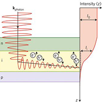 | MB Johnston
Nat. Photonics, 11:268-269 (May 2017)
[
pdf ][ SI ][ ref ]
There is typically a compromise between speed and efficiency when designing silicon photodiodes. Now, researchers have exploited microstructuring to achieve fast and thin devices that are also efficient.
Citations: 12 (Scopus) 11 (Web of Science) |
- An ultrafast switchable terahertz polarization modulator based on iii-v semiconductor nanowires
-
 | SA Baig, JL Boland, DA Damry, HH Tan, C Jagadish, HJ Joyce, MB Johnston
Nano Lett., 17:2603-2610 (Apr 2017)
[
pdf ][ SI ][ ref ]
Progress in the terahertz (THz) region of the electromagnetic spectrum is undergoing major advances, with advanced THz sources and detectors being developed at a rapid pace. Yet, ultrafast THz communication is still to be realized, owing to the lack of practical and effective THz modulators. Here, we present a novel ultrafast active THz polarization modulator based on GaAs semiconductor nanowires arranged in a wire-grid configuration. We utilize an optical pump-terahertz probe spectroscopy system and vary the polarization of the optical pump beam to demonstrate ultrafast THz modulation with a switching time of less than 5 ps and a modulation depth of -8 dB. We achieve an extinction of over 13% and a dynamic range of -9 dB, comparable to microsecond-switchable graphene- and metamaterial-based THz modulators, and surpassing the performance of optically switchable carbon nanotube THz polarizers. We show a broad bandwidth for THz modulation between 0.1 and 4 THz. Thus, this work presents the first THz modulator which combines not only a large modulation depth but also a broad bandwidth and picosecond time resolution for THz intensity and phase modulation, making it an ideal candidate for ultrafast THz communication.
Citations: 89 (Scopus) 87 (Web of Science) |
- Single $n^+$-i-$n^+$ {InP} nanowires for highly sensitive terahertz detection
-
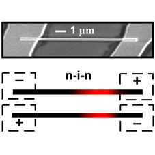 | K Peng, P Parkinson, Q Gao, JL Boland, ZY Li, F Wang, S Mokkapati, L Fu, MB Johnston, HH Tan, C Jagadish
Nanotechnology, 28:125202 (Mar 2017)
[
pdf ][ SI ][ ref ]
Developing single-nanowire terahertz (THz) electronics and employing them as sub-wavelength components for highly-integrated THz time-domain spectroscopy (THz-TDS) applications is a promising approach to achieve future low-cost, highly integrable and high-resolution THz tools, which are desirable in many areas spanning from security, industry, environmental monitoring and medical diagnostics to fundamental science. In this work, we present the design and growth of n(+)-i-n(+) InP nanowires. The axial doping profile of the n+-i-n+ InP nanowires has been calibrated and characterized using combined optical and electrical approaches to achieve nanowire devices with low contact resistances, on which the highly-sensitive InP singlenanowire photoconductive THz detectors have been demonstrated. While the n+-i-n+ InP nanowire detector has a only pA-level response current, it has a 2.5 times improved signal-tonoise ratio compared with the undoped InP nanowire detector and is comparable to traditional bulk THz detectors. This performance indicates a promising path to nanowire-based THz electronics for future commercial applications.
Citations: 33 (Scopus) 29 (Web of Science) |
- The 2017 terahertz science and technology roadmap
-
 | SS Dhillon, MS Vitiello, EH Linfield, AG Davies, MC Hoffmann, MB Johnston
J. Phys. D-Appl. Phys., 50:043001 (Feb 2017)
[
pdf ][ SI ][ ref ]
Science and technologies based on terahertz frequency electromagnetic radiation (100 GHz-30 THz) have developed rapidly over the last 30 years. For most of the 20th Century, terahertz radiation, then referred to as sub-millimeter wave or far-infrared radiation, was mainly utilized by astronomers and some spectroscopists. Following the development of laser based terahertz time-domain spectroscopy in the 1980s and 1990s the field of THz science and technology expanded rapidly, to the extent that it now touches many areas from fundamental science to \'real world\' applications. For example THz radiation is being used to optimize materials for new solar cells, and may also be a key technology for the next generation of airport security scanners. While the field was emerging it was possible to keep track of all new developments, however now the field has grown so much that it is increasingly difficult to follow the diverse range of new discoveries and applications that are appearing. At this point in time, when the field of THz science and technology is moving from an emerging to a more established and interdisciplinary field, it is apt to present a roadmap to help identify the breadth and future directions of the field. The aim of this roadmap is to present a snapshot of the present state of THz science and technology in 2017, and provide an opinion on the challenges and opportunities that the future holds. To be able to achieve this aim, we have invited a group of international experts to write 18 sections that cover most of the key areas of THz science and technology. We hope that The 2017 Roadmap on THz science and technology will prove to be a useful resource by providing a wide ranging introduction to the capabilities of THz radiation for those outside or just entering the field as well as providing perspective and breadth for those who are well established. We also feel that this review should serve as a useful guide for government and funding agencies.
Citations: 1399 (Scopus) 1271 (Web of Science) |
- Influence of Interface Morphology on Hysteresis in Vapor-Deposited Perovskite Solar Cells
-
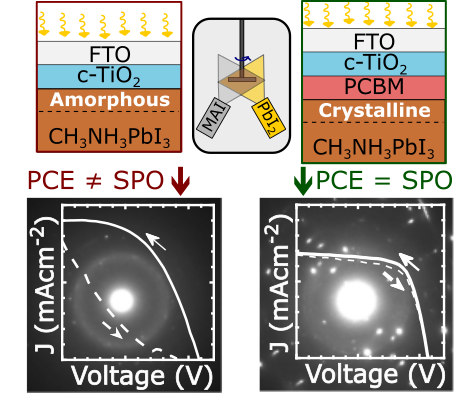 | JB Patel, J Wong-Leung, S Van Reenen, N Sakai, JTW Wang, ES Parrott, M Liu, HJ Snaith, LM Herz, MB Johnston
Adv. Electron. Mater., 3:1600470 (Feb 2017)
[
pdf ][ SI ][ ref ]
Hysteresis in the current–voltage characteristics of vapor‐deposited perovskite solar cells is shown to originate from an amorphous region of CH3NH3PbI3 at the interface with the device's electron transport layer. Interface engineering is used to produce highly crystalline perovskite material at this interface which results in hysteresis‐free evaporated planar heterojunction solar cells.
Citations: 66 (Scopus) 64 (Web of Science) |
- {Cs}$_2${InAgCl}$_6$: a new lead-free halide double perovskite with direct band gap
-
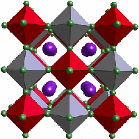 | G Volonakis, AA Haghighirad, RL Milot, WH Sio, MR Filip, B Wenger, MB Johnston, LM Herz, HJ Snaith, F Giustino
J. Phys. Chem. Lett., 8:772- (Feb 2017)
[
pdf ][ SI ][ ref ]
A(2)BB\'X-6 halide double perovskites based on bismuth and silver have recently been proposed as potential environmentally friendly alternatives to lead-based hybrid halide perovskites. In particular, Cs2BiAgX6 (X = Cl, Br) have been synthesized and found to exhibit band gaps in the visible range. However, the band gaps of these compounds are indirect, which is not ideal for applications in thin film photovoltaics. Here, we propose a new class of halide double perovskites, where the B3+ and B+ cations are In3+ and Ag+, respectively. Our first-principles calculations indicate that the hypothetical compounds Cs2InAgX6 (X = Cl, Br, I) should exhibit direct band gaps between the visible (I) and the ultraviolet (Cl). Based on these predictions, we attempt to synthesize Cs2InAgCl6 and Cs2InAgBr6, and we succeed to form the hitherto unknown double perovskite Cs2InAgCl6. X-ray diffraction yields a double perovskite structure with space group Fm3m. The measured band gap is 3.3 eV, and the compound is found to be photosensitive and turns reversibly from white to orange under ultraviolet illumination. We also perform an empirical analysis of the stability of Cs2InAgX6 and their mixed halides based on Goldschmidts rules, and we find that it should also be possible to form Cs2InAg(Cl1xBrx)(6) for x < 1. The synthesis of mixed halides will open the way to the development of lead-free double perovskites with direct and tunable band gaps.
Citations: 1019 (Scopus) 987 (Web of Science) |
- Efficient and air-stable mixed-cation lead mixed-halide perovskite solar cells with n-doped organic electron extraction layers
-
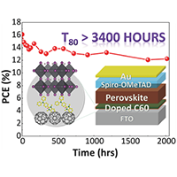 | ZP Wang, DP McMeekin, N Sakai, K Wojciechowski, JB Patel, MB Johnston, HJ Snaith
Adv. Mater., 29:UNSP 1604186 (Feb 2017)
[
pdf ][ SI ][ ref ]
Air-stable doping of the n-type fullerene layer in an n-i-p planar heterojunction perovskite device is capable of enhancing device efficiency and improving device stability. Employing a (HC(NH2)(2))(0.83)Cs0.17Pb(I0.6Br0.4)(3) perovskite as the photoactive layer, glass-glass laminated devices are reported, which sustain 80% of their \"post burn-in\" efficiency over 3400 h under full sun illumination in ambient conditions.
Citations: 293 (Scopus) 216 (Web of Science) |
- A low viscosity, low boiling point, clean solvent system for the rapid crystallisation of highly specular perovskite films
-
 | NK Noel, SN Habisreutinger, B Wenger, MT Klug, MT Horantner, MB Johnston, RJ Nicholas, DT Moore, HJ Snaith
Energy Environ. Sci., 10:145-152 (Jan 2017)
[
pdf ][ SI ][ ref ]
Perovskite-based photovoltaics have, in recent years, become poised to revolutionise the solar industry. While there have been many approaches taken to the deposition of this material, one-step spin-coating remains the simplest and most widely used method in research laboratories. Although spin-coating is not recognised as the ideal manufacturing methodology, it represents a starting point from which more scalable deposition methods, such as slot-dye coating or ink-jet printing can be developed. Here, we introduce a new, low-boiling point, low viscosity solvent system that enables rapid, room temperature crystallisation of methylammonium lead triiodide perovskite films, without the use of strongly coordinating aprotic solvents. Through the use of this solvent, we produce dense, pinhole free films with uniform coverage, high specularity, and enhanced optoelectronic properties. We fabricate devices and achieve stabilised power conversion efficiencies of over 18% for films which have been annealed at 100 degrees C, and over 17% for films which have been dried under vacuum and have undergone no thermal processing. This deposition technique allows uniform coating on substrate areas of up to 125 cm(2), showing tremendous promise for the fabrication of large area, high efficiency, solution processed devices, and represents a critical step towards industrial upscaling and large area printing of perovskite solar cells.
Citations: 386 (Scopus) 373 (Web of Science) |
- Photovoltaic mixed-cation lead mixed-halide perovskites: links between crystallinity, photo-stability and electronic properties
-
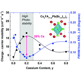 | W Rehman, DP McMeekin, JB Patel, RL Milot, MB Johnston, HJ Snaith, LM Herz
Energy Environ. Sci., 10:361-369 (Jan 2017)
[
pdf ][ SI ][ ref ]
Lead mixed halide perovskites are highly promising semiconductors for both multi-junction photovoltaic and light emitting applications due to their tunable band gaps, with emission and absorption energies spanning the UV-visible to near IR regions. However, many such perovskites exhibit unwanted halide segregation under photo-illumination, the cause of which is still unclear. In our study, we establish crucial links between crystal phase stability, photostability and optoelectronic properties of the mixed-cation lead mixed-halide perovskite Cs(y)FA((1-y)) Pb(BrxI(1-x))(3). We demonstrate a region for caesium content between 0.10 < y < 0.30 which features high crystalline quality, long charge-carrier lifetimes and high charge-carrier mobilities. Importantly, we show that for such high-quality perovskites, photo-induced halide segregation is strongly suppressed, suggesting that high crystalline quality is a prerequisite for good optoelectronic quality and band gap stability. We propose that regions of short-range crystalline order aid halide segregation, possibly by releasing lattice strain between iodide rich and bromide rich domains. For an optimized caesium content, we explore the orthogonal halide-variation parameter space for Cs(0.17)FA(0.83)Pb(BrxI(1-x))(3) perovskites. We demonstrate excellent charge-carrier mobilities (11-40 cm(2) V-1 s(-1)) and diffusion lengths (0.8-4.4 mm) under solar conditions across the full iodide-bromide tuning range. Therefore, the addition of caesium yields a more photo-stable perovskite system whose absorption onsets can be tuned for bandgap-optimized tandem solar cells.
Citations: 569 (Scopus) 552 (Web of Science) |
- Charge-carrier dynamics in {2D} hybrid metal-halide perovskites
-
 | RL Milot, RJ Sutton, GE Eperon, AA Haghighirad, JM Hardigree, L Miranda, HJ Snaith, MB Johnston, LM Herz
Nano Lett., 16:7001 (Nov 2016)
[
pdf ][ SI ][ ref ]
Hybrid metal-halide perovskites are promising new materials for use in solar cells; however, their chemical stability in the presence of moisture remains a significant drawback. Quasi two-dimensional (2D) perovskites that incorporate hydrophobic organic interlayers offer improved resistance to degradation by moisture, currently still at the cost of overall cell efficiency. To elucidate the factors affecting the optoelectronic properties of these materials, we have investigated the charge transport properties and crystallographic orientation of mixed methylammonium (MA)-phenylethylammonium (PEA) lead iodide thin films as a function of the MA-to-PEA ratio and, thus, the thickness of the \"encapsulated\" MA lead halide layers. We find that monomolecular charge-carrier recombination rates first decrease with increasing PEA fraction, most likely as a result of trap passivation, but then increase significantly as excitonic effects begin to dominate for thin confined layers. Bimolecular and Auger recombination rate constants are found to be sensitive to changes in electronic confinement, which alters the density of states for electronic transitions. We demonstrate that effective charge-carrier mobilities remain remarkably high (near 10 cm(2)V-(1)s(-1)) for intermediate PEA content and are enhanced for preferential orientation of the conducting lead iodide layers along the probing electric field. The trade-off between trap reduction, electronic confinement, and layer orientation leads to calculated charge-carrier diffusion lengths reaching a maximum of 2.5 mu m for intermediate PEA content (50%).
Citations: 493 (Scopus) 478 (Web of Science) |
- A review of the electrical properties of semiconductor nanowires: insights gained from terahertz conductivity spectroscopy
-
 | HJ Joyce, JL Boland, CL Davies, SA Baig, MB Johnston
Semicond. Sci. Technol., 31:103003 (Oct 2016)
[
pdf ][ SI ][ ref ]
Accurately measuring and controlling the electrical properties of semiconductor nanowires is of paramount importance in the development of novel nanowire-based devices. In light of this, terahertz. (THz) conductivity spectroscopy has emerged as an ideal non-contact technique for probing nanowire electrical conductivity and is showing tremendous value in the targeted development of nanowire devices. THz spectroscopic measurements of nanowires enable charge carrier lifetimes, mobilities, dopant concentrations and surface recombination velocities to be measured with high accuracy and high throughput in a contact-free fashion. This review spans seminal and recent studies of the electronic properties of nanowires using THz spectroscopy. A didactic description of THz time-domain spectroscopy, optical pump-THz probe spectroscopy, and their application to nanowires is included. We review a variety of technologically important nanowire materials, including GaAs, InAs, InP, GaN and InN nanowires, Si and Ge nanowires, ZnO nanowires, nanowire heterostructures, doped nanowires and modulation-doped nanowires. Finally, we discuss how THz measurements are guiding the development of nanowire-based devices, with the example of single-nanowire photoconductive THz receivers.
Citations: 225 (Scopus) 215 (Web of Science) |
- Radiative monomolecular recombination boosts amplified spontaneous emission in $HC(NH_2)_2SnI_3$ perovskite films
-
 | RL Milot, GE Eperon, T Green, HJ Snaith, MB Johnston, LM Herz
J. Phys. Chem. Lett., 7:4178-4184 (Oct 2016)
[
pdf ][ SI ][ ref ]
Hybrid metal-halide perovskites have potential as cost-effective gain media for laser technology because of their superior optoelectronic properties. Although lead-halide perovskites have been most widely studied to date, tin-based perovskites have been proposed as a less toxic alternative. In this Letter, we show that amplified spontaneous emission (ASE) in formamidinium tin triiodide (FASnI(3)) thin films is supported by an observed radiative monomolecular charge recombination pathway deriving from its unintentional doping. Such a radiative component will be active even at the lowest charge-carrier densities, opening a pathway for ultralow light-emission thresholds. Using time-resolved THz photoconductivity analysis, we further show that the material has an unprecedentedly high charge-carrier mobility of 22 cm(2) V-1 s(-1) favoring efficient transport. In addition, FASnI(3) exhibits strong radiative bimolecular recombination and Auger rates that are over an order of magnitude lower than for lead halide perovskites. In combination, these properties reveal that tin-halide perovskites are highly suited to light-emitting devices.
Citations: 138 (Scopus) 133 (Web of Science) |
- Broadband phase-sensitive single {InP} nanowire photoconductive terahertz detectors
-
 | K Peng, P Parkinson, JL Boland, Q Gao, YC Wenas, CL Davies, ZY Li, L Fu, MB Johnston, HH Tan, C Jagadish
Nano Lett., 16:4925-4931 (Aug 2016)
[
pdf ][ SI ][ ref ]
Terahertz time-domain spectroscopy (THz-TDS) has emerged as a powerful tool for materials characterization and imaging. A trend toward size reduction, higher component integration, and performance improvement for advanced THz-TDS systems is of increasing interest. The use of single semiconducting nanowires for terahertz (THz) detection is a nascent field that has great potential to realize future highly integrated THz systems. In order to develop such components, optimized material optoelectronic properties and careful device design are necessary. Here, we present antenna-optimized photoconductive detectors based on single InP nanowires with superior properties of high carrier mobility (similar to 1260 cm(2) V-1 s(-1)) and low dark current (similar to 10 pA), which exhibit excellent sensitivity and broadband performance. We demonstrate that these nanowire THz detectors can provide high quality time-domain spectra for materials characterization in a THz-TDS system, a critical step toward future application in advanced THz-TDS system with high spectral and spatial resolution.
Citations: 60 (Scopus) 55 (Web of Science) |
- Electron-phonon coupling in hybrid lead halide perovskites
-
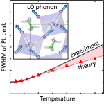 | AD Wright, C Verdi, RL Milot, GE Eperon, MA Pérez-Osorio, HJ Snaith, F Giustino, MB Johnston, LM Herz
Nat. Commun., 7:11755 (May 2016)
[
pdf ][ SI ][ ref ]
Phonon scattering limits charge-carrier mobilities and governs emission line broadening in hybrid metal halide perovskites. Establishing how charge carriers interact with phonons in these materials is therefore essential for the development of high-efficiency perovskite photovoltaics and low-cost lasers. Here we investigate the temperature dependence of emission line broadening in the four commonly studied formamidinium and methylammonium perovskites, HC(NH2)(2)PbI3, HC(NH2)(2)PbBr3, CH3NH3PbI3 and CH3NH3PbBr3, and discover that scattering from longitudinal optical phonons via the Frohlich interaction is the dominant source of electron-phonon coupling near room temperature, with scattering off acoustic phonons negligible. We determine energies for the interacting longitudinal optical phonon modes to be 11.5 and 15.3 meV, and Frohlich coupling constants of similar to 40 and 60 meV for the lead iodide and bromide perovskites, respectively. Our findings correlate well with first-principles calculations based on many-body perturbation theory, which underlines the suitability of an electronic band-structure picture for describing charge carriers in hybrid perovskites.
Citations: 1207 (Scopus) 1202 (Web of Science) |
- Bandgap-tunable cesium lead halide perovskites with high thermal stability for efficient solar cells
-
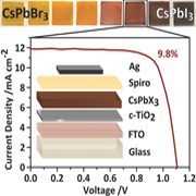 | RJ Sutton, GE Eperon, L Miranda, ES Parrott, BA Kamino, JB Patel, MT Horantner, MB Johnston, AA Haghighirad, DT Moore, HJ Snaith
Adv. Energy Mater., 6:1502458 (Apr 2016)
[
pdf ][ SI ][ ref ]
Highest reported efficiency cesium lead halide perovskite solar cells are realized by tuning the bandgap and stabilizing the black perovskite phase at lower temperatures. CsPbI2Br is employed in a planar architecture device resulting in 9.8% power conversion efficiency and over 5% stabilized power output. Offering substantially enhanced thermal stability over their organic based counterparts, these results show that all-inorganic perovskites can represent a promising next step for photovoltaic materials.
Citations: 1464 (Scopus) 1434 (Web of Science) |
- Effect of structural phase transition on charge-carrier lifetimes and defects in ch3nh3sni3 perovskite
-
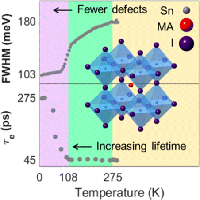 | ES Parrott, RL Milot, T Stergiopoulos, HJ Snaith, MB Johnston, LM Herz
J. Phys. Chem. Lett., 7:1321-1326 (Apr 2016)
[
pdf ][ SI ][ ref ]
Methylammonium tin triiodide (MASnI(3)) has been successfully employed in lead-free perovskite solar cells, but overall power-conversion efficiencies are still significantly lower than for lead-based perovskites. Here we present photoluminescence (PL) spectra and time resolved PL from 8 to 295 K and find a marked improvement in carrier lifetime and a substantial reduction in PL line width below similar to 110 K, indicating that the cause of the hindered performance is activated at the orthorhombic to tetragonal phase transition. Our measurements therefore suggest that targeted structural change may be capable of tailoring the relative energy level alignment of defects (e.g., tin vacancies) to reduce the background dopant density and improve charge extraction. In addition, we observe for the first time an above-gap emission feature that may arise from higher-lying interband transitions, raising the prospect of excess energy harvesting.
Citations: 160 (Scopus) 161 (Web of Science) |
- Increased Photoconductivity Lifetime in GaAs Nanowires by Controlled n-Type and p-Type Doping
-
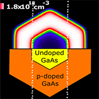 | JL Boland, A Casadei, G Tutuncuoglu, F Matteini, CL Davies, F Jabeen, HJ Joyce, LM Herz, A Fontcuberta i Morral, MB Johnston
ACS Nano, 10:4219-4227 (Mar 2016)
[
pdf ][ SI ][ ref ]
Controlled doping of GaAs nanowires is crucial for the development of nanowire-based electronic and optoelectronic devices. Here, we present a noncontact method based on time-resolved terahertz photoconductivity for assessing n- and p-type doping efficiency in nanowires. Using this technique, we measure extrinsic electron and hole concentrations in excess of 1018 cm–3 for GaAs nanowires with n-type and p-type doped shells. Furthermore, we show that controlled doping can significantly increase the photoconductivity lifetime of GaAs nanowires by over an order of magnitude: from 0.13 ns in undoped nanowires to 3.8 and 2.5 ns in n-doped and p-doped nanowires, respectively. Thus, controlled doping can be used to reduce the effects of parasitic surface recombination in optoelectronic nanowire devices, which is promising for nanowire devices, such as solar cells and nanowire lasers.
Citations: 66 (Scopus) 64 (Web of Science) |
- Structured organic-inorganic perovskite toward a distributed feedback laser
-
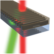 | M Saliba, SM Wood, JB Patel, PK Nayak, J Huang, JA Alexander-webber, B Wenger, SD Stranks, MT Horantner, JTW Wang, RJ Nicholas, LM Herz, MB Johnston, SM Morris, HJ Snaith, MK Riede
Adv. Mater., 28:923-929 (Feb 2016)
[
pdf ][ SI ][ ref ]
A general strategy for the in-plane structuring of organic–inorganic perovskite films is presented. The method is used to fabricate an industrially relevant distributed feedback (DFB) cavity, which is a critical step toward all-electrially pumped injection laser diodes. This approach opens the prospects of perovskite materials for much improved optical control in LEDs, solar cells, and also toward applications as optical devices.
Citations: 292 (Scopus) 267 (Web of Science) |
- Hybrid Perovskites for Photovoltaics: Charge-Carrier Recombination, Diffusion, and Radiative Efficiencies
-
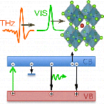 | MB Johnston, LM Herz
Accounts Chem. Res., 49:146--154 (Jan 2016)
[
pdf ][ SI ][ ref ]
Photovoltaic (PV) devices that harvest the energy provided by the sun have great potential as renewable energy sources, yet uptake has been hampered by the increased cost of solar electricity compared with fossil fuels. Hybrid metal halide perovskites have recently emerged as low-cost active materials in PV cells with power conversion efficiencies now exceeding 20%. Rapid progress has been achieved over only a few years through improvements in materials processing and device design. In addition, hybrid perovskites appear to be good light emitters under certain conditions, raising the prospect of applications in low-cost light-emitting diodes and lasers.
Citations: 1004 (Scopus) 958 (Web of Science) |
- Formation Dynamics of CH$_3$NH$_3$PbI$_3$ Perovskite Following Two-Step Layer Deposition
-
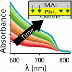 | JB Patel, RL Milot, AD Wright, LM Herz, MB Johnston
J. Phys. Chem. Lett., 7:96-102 (Jan 2016)
[
pdf ][ SI ][ ref ]
Hybrid metal-halide perovskites have emerged as a leading class of semiconductors for optoelectronic devices because of their desirable material properties and versatile fabrication methods. However, little is known about the chemical transformations that occur in the initial stages of perovskite crystal formation. Here we follow the real-time formation dynamics of MAPbI3 from a bilayer of lead iodide (PbI2) and methylammonium iodide (MAI) deposited through a two-step thermal evaporation process. By lowering the substrate temperature during deposition, we are able to initially inhibit intermixing of the two layers. We subsequently use infrared and visible light transmission, X-ray diffraction, and photoluminescence lifetime measurements to reveal the room-temperature transformations that occur in vacuum and ambient air, as MAI diffuses into the PbI2 lattice to form MAPbI3. In vacuum, the transformation to MAPbI3 is incomplete as unreacted MAI is retained in the film. However, exposure to moist air allows for conversion of the unreacted MAI to MAPbI3, demonstrating that moisture is essential in making MAI more mobile and thus aiding perovskite crystallization. These dynamic processes are reflected in the observed charge-carrier lifetimes, which strongly fluctuate during periods of large ion migration but steadily increase with improving crystallinity.
Citations: 118 (Scopus) 110 (Web of Science) |
- A mixed-cation lead mixed-halide perovskite absorber for tandem solar cells
-
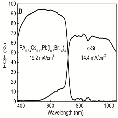 | DP McMeekin, G Sadoughi, W Rehman, GE Eperon, M Saliba, MT Hörantner, A Haghighirad, N Sakai, L Korte, B Rech, MB Johnston, LM Herz, HJ Snaith
Science, 351:151-155 (Jan 2016)
[
pdf ][ SI ][ ref ]
Metal halide perovskite photovoltaic cells could potentially boost the efficiency of commercial silicon photovoltaic modules from ∼20 toward 30% when used in tandem architectures. An optimum perovskite cell optical band gap of ~1.75 electron volts (eV) can be achieved by varying halide composition, but to date, such materials have had poor photostability and thermal stability. Here we present a highly crystalline and compositionally photostable material, [HC(NH2)2]0.83Cs0.17Pb(I0.6Br0.4)3, with an optical band gap of ~1.74 eV, and we fabricated perovskite cells that reached open-circuit voltages of 1.2 volts and power conversion efficiency of over 17% on small areas and 14.7% on 0.715 cm2 cells. By combining these perovskite cells with a 19%-efficient silicon cell, we demonstrated the feasibility of achieving >25%-efficient four-terminal tandem cells.
Citations: 2840 (Scopus) 2743 (Web of Science) |
- Efficient perovskite solar cells by metal ion doping
-
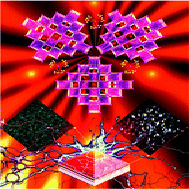 | JTW Wang, ZP Wang, S Pathak, W Zhang, DW Dequilettes, F Wisnivesky-rocca-rivarola, J Huang, PK Nayak, JB Patel, HAM Yusof, Y Vaynzof, R Zhu, I Ramirez, J Zhang, C Ducati, C Grovenor, MB Johnston, DS Ginger, RJ Nicholas, HJ Snaith
Energy Environ. Sci., 9:2892-2901 ( 2016)
[
pdf ][ SI ][ ref ]
Realizing the theoretical limiting power conversion efficiency (PCE) in perovskite solar cells requires a better understanding and control over the fundamental loss processes occurring in the bulk of the perovskite layer and at the internal semiconductor interfaces in devices. One of the main challenges is to eliminate the presence of charge recombination centres throughout the film which have been observed to be most densely located at regions near the grain boundaries. Here, we introduce aluminium acetylacetonate to the perovskite precursor solution, which improves the crystal quality by reducing the microstrain in the polycrystalline film. At the same time, we achieve a reduction in the non-radiative recombination rate, a remarkable improvement in the photoluminescence quantum efficiency (PLQE) and a reduction in the electronic disorder deduced from an Urbach energy of only 12.6 meV in complete devices. As a result, we demonstrate a PCE of 19.1% with negligible hysteresis in planar heterojunction solar cells comprising all organic p and n-type charge collection layers. Our work shows that an additional level of control of perovskite thin film quality is possible via impurity cation doping, and further demonstrates the continuing importance of improving the electronic quality of the perovskite absorber and the nature of the heterojunctions to further improve the solar cell performance.
Citations: 439 (Scopus) 416 (Web of Science) |
- Enhanced uv-light stability of planar heterojunction perovskite solar cells with caesium bromide interface modification
-
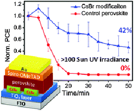 | WZ Li, W Zhang, RJ Sutton, JD Fan, AA Haghighirad, MB Johnston, LD Wang, HJ Snaith
Energy Environ. Sci., 9:490-498 ( 2016)
[
pdf ][ SI ][ ref ]
Interfacial engineering has been shown to play a vital role in boosting the performance of perovskite solar cells in the past few years. Here we demonstrate that caesium bromide (CsBr), as an interfacial modifier between the electron collection layer and the CH3NH3PbI3-xClx absorber layer, can effectively enhance the stability of planar heterojunction devices under ultra violet (UV) light soaking. Additionally, the device performance is improved due to the alleviated defects at the perovskite-titania heterojunction and enhanced electron extraction.
Citations: 600 (Scopus) 573 (Web of Science) |
- Low Ensemble Disorder in Quantum Well Tube Nanowires
-
 | CL Davies, P Parkinson, N Jiang, JL Boland, S Conesa-Boj, HH Tan, C Jagadish, LM Herz, MB Johnston
Nanoscale, 7:20531--20538 (Dec 2015)
[
pdf ][ SI ][ ref ]
We have observed very low disorder in high quality quantum well tubes (QWT) in GaAs-Al$_{0.44}$Ga$_{0.56}$As core-multishell nanowires. Room-temperature photoluminescence spectra were measured from 150 single nanowires enabling a full statistical analysis of both intra- and inter-nanowire disorder. By modelling individual nanowire spectra{,} we assigned a quantum well tube thickness{,} a core disorder parameter and a QWT disorder parameter to each nanowire. A strong correlation was observed between disorder in the GaAs cores and disorder in the GaAs QWTs{,} which indicates that variations in core morphology effectively propagate to the shell layers. This highlights the importance of high quality core growth prior to shell deposition. Furthermore{,} variations in QWT thicknesses for different facet directions was found to be a likely cause of intra-wire disorder{,} highlighting the need for accurate shell growth
Citations: 14 (Scopus) 15 (Web of Science) |
- Charge-Carrier Dynamics and Mobilities in Formamidinium Lead Mixed-Halide Perovskites
-
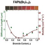 | W Rehman, RL Milot, GE Eperon, C Wehrenfennig, JL Boland, HJ Snaith, MB Johnston, LM Herz
Adv. Mater., 27:7938--7944 (Dec 2015)
[
pdf ][ SI ][ ref ]
The mixed-halide perovskite FAPb(BryI1–y)3 is attractive for color-tunable and tandem solar cells. Bimolecular and Auger charge-carrier recombination rate constants strongly correlate with the Br content, y, suggesting a link with electronic structure. FAPbBr3 and FAPbI3 exhibit charge-carrier mobilities of 14 and 27 cm2 V−1 s−1 and diffusion lengths exceeding 1 μm, while mobilities across the mixed Br/I system depend on crystalline phase disorder.
Citations: 418 (Scopus) 396 (Web of Science) |
- Colour-selective photodiodes
-
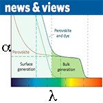 | MB Johnston
Nat. Photonics, 9:633-636 (Oct 2015)
[
pdf ][ SI ][ ref ]
Perovskite semiconductors have altered the landscape of solar cell research. Now researchers show that these materials may also offer a flexible platform for colour imaging and wavelength-selective sensing.
Citations: 43 (Scopus) 41 (Web of Science) |
- Temperature-dependent charge-carrier dynamics in {CH$_3$NH$_3$PbI$_3$} perovskite thin films
-
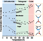 | RL Milot, GE Eperon, HJ Snaith, MB Johnston, LM Herz
Adv. Funct. Mater., 25:6218-6227 (Oct 2015)
[
pdf ][ SI ][ ref ]
The photoluminescence, transmittance, charge-carrier recombination dynamics, mobility, and diffusion length of CH3NH3PbI3 are investigated in the temperature range from 8 to 370 K. Profound changes in the optoelectronic properties of this prototypical photovoltaic material are observed across the two structural phase transitions occurring at 160 and 310 K. Drude-like terahertz photoconductivity spectra at all temperatures above 80 K suggest that charge localization effects are absent in this range. The monomolecular charge-carrier recombination rate generally increases with rising temperature, indicating a mechanism dominated by ionized impurity mediated recombination. Deduced activation energies E-a associated with ionization are found to increase markedly from the room-temperature tetragonal (E-a approximate to 20 meV) to the higher-temperature cubic (E-a approximate to 200 meV) phase adopted above 310 K. Conversely, the bimolecular rate constant decreases with rising temperature as charge-carrier mobility declines, while the Auger rate constant is highly phase specific, suggesting a strong dependence on electronic band structure. The charge-carrier diffusion length gradually decreases with rising temperature from about 3 m at -93 degrees C to 1.2 m at 67 degrees C but remains well above the optical absorption depth in the visible spectrum. These results demonstrate that there are no fundamental obstacles to the operation of cells based on CH3NH3PbI3 under typical field conditions.
Citations: 915 (Scopus) 877 (Web of Science) |
- Vibrational Properties of the Organic−Inorganic Halide Perovskite $CH_3NH_3PbI_3$ from Theory and Experiment: Factor Group Analysis, First-Principles Calculations, and Low-Temperature Infrared Spectra
-
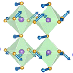 | MA Perez-Osorio, RL Milot, MR Filip, JB Patel, LM Herz, MB Johnston, F Giustino
J. Phys. Chem. C, 119:25703--25718 (Oct 2015)
[
pdf ][ SI ][ ref ]
In this work, we investigate the vibrational
properties of the hybrid organic/inorganic halide perovskite
MAPbI3 (MA = CH3NH3) in the range 6−3500 cm−1 by
combining first-principles density-functional perturbation
theory calculations and low-temperature infrared (IR)
absorption measurements on evaporated perovskite films. By
using a group factor analysis, we establish the symmetry of the
normal modes of vibration and predict their IR and Raman
activity. We validate our analysis via explicit calculation of the
IR intensities. Our calculated spectrum is in good agreement
with our measurements. By comparing theory and experiment,
we are able to assign most of the features in the IR spectrum.
Our analysis shows that the IR spectrum of MAPbI3 can be
partitioned into three distinct regions: the internal vibrations of the MA cations (800−3100 cm 180 cm−1), and the internal vibrations of the PbI3 network (<100 cm−1). The low-frequency region of the IR spectrum is dominated by Pb−I stretching modes of the PbI3 network with Bu symmetry and librational modes of the MA cations. In addition, we find that the largest contributions to the static dielectric constant arise from Pb−I stretching and Pb−I−Pb rocking modes, and that one low-frequency B2u Pb−I stretching mode exhibits a large LO−TO splitting of 50 cm−1.
Citations: 334 (Scopus) 327 (Web of Science) |
- Plasmonic-induced photon recycling in metal halide perovskite solar cells
-
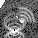 | M Saliba, W Zhang, VM Burlakov, SD Stranks, Y Sun, JM Ball, MB Johnston, A Goriely, U Wiesner, HJ Snaith
Adv. Funct. Mater., 25:5038-5046 (Aug 2015)
[
pdf ][ SI ][ ref ]
Organic-inorganic metal halide perovskite solar cells have emerged in the past few years to promise highly efficient photovoltaic devices at low costs. Here, temperature-sensitive core-shell Ag@TiO2 nanoparticles are successfully incorporated into perovskite solar cells through a low-temperature processing route, boosting the measured device efficiencies up to 16.3%. Experimental evidence is shown and a theoretical model is developed which predicts that the presence of highly polarizable nanoparticles enhances the radiative decay of excitons and increases the reabsorption of emitted radiation, representing a novel photon recycling scheme. The work elucidates the complicated subtle interactions between light and matter in plasmonic photovoltaic composites. Photonic and plasmonic schemes such as this may help to move highly efficient perovskite solar cells closer to the theoretical limiting efficiencies.
Citations: 218 (Scopus) 209 (Web of Science) |
- Enhanced amplified spontaneous emission in perovskites using a flexible cholesteric liquid crystal reflector
-
 | SD Stranks, SM Wood, K Wojciechowski, F Deschler, M Saliba, H Khandelwal, JB Patel, SJ Elston, LM Herz, MB Johnston, APHJ Schenning, MG Debije, MK Riede, SM Morris, HJ Snaith
Nano Lett., 15:4935-4941 (May 2015)
[
pdf ][ SI ][ ref ]
Organic-inorganic perovskites are highly promising solar cell materials with laboratory-based power conversion efficiencies already matching those of established thin film technologies. Their exceptional photovoltaic performance is in part attributed to the presence of efficient radiative recombination pathways, thereby opening up the possibility of efficient light-emitting devices. Here, we demonstrate optically pumped amplified spontaneous emission (ASE) at 780 urn from a 50 nm-thick film of CH3NH3PbI3 perovskite that is sandwiched within a cavity composed of a thin-film (similar to 7 mu m) cholesteric liquid crystal (CLC) reflector and a metal back-reflector. The threshold fluence for ASE in the perovskite film is reduced by at least two orders of magnitude in the presence of the CLC reflector, which results in a factor of two reduction in threshold fluence compared to previous reports. We consider this to be due to improved coupling of the oblique and out-of-plane modes that are reflected into the bulk in addition to any contributions from cavity modes. Furthermore, we also demonstrate enhanced ASE on flexible reflectors and discuss how improvements in the quality factor and reflectivity of the CLC layers could lead to single-mode lasing using CLC reflectors. Our work opens up the possibility of fabricating widely wavelength-tunable \"mirror-less\" single-mode lasers on flexible substrates, which could find use in applications such as flexible displays and friend or foe identification.
Citations: 129 (Scopus) 122 (Web of Science) |
- {In$_x$Ga$_{1-x}$As} nanowires with uniform composition, pure wurtzite crystal phase and taper-free morphology
-
 | AS Ameruddin, HA Fonseka, P Caroff, J Wong-leung, RLMOH Veld, JL Boland, MB Johnston, HH Tan, C Jagadish
Nanotechnology, 26:205604 (May 2015)
[
pdf ][ SI ][ ref ]
Obtaining compositional homogeneity without compromising morphological or structural quality is one of the biggest challenges in growing ternary alloy compound semiconductor nanowires. Here we report growth of Au-seeded InxGa1-xAs nanowires via metal-organic vapour phase epitaxy with uniform composition, morphology and pure wurtzite (WZ) crystal phase by carefully optimizing growth temperature and V/III ratio. We find that high growth temperatures allow the InxGa1-xAs composition to be more uniform by suppressing the formation of typically observed spontaneous In-rich shells. A low V/III ratio results in the growth of pure WZ phase InxGa1-xAs nanowires with uniform composition and morphology while a high V/III ratio allows pure zinc-blende (ZB) phase to form. Ga incorporation is found to be dependent on the crystal phase favouring higher Ga concentration in ZB phase compared to the WZ phase. Tapering is also found to be more prominent in defective nanowires hence it is critical to maintain the highest crystal structure purity in order to minimize tapering and inhomogeneity. The InP capped pure WZ In0.65Ga0.35As core-shell nanowire heterostructures show 1.54 mu m photoluminescence, close to the technologically important optical fibre telecommunication wavelength, which is promising for application in photodetectors and nanoscale lasers.
Citations: 41 (Scopus) 40 (Web of Science) |
- Charge selective contacts, mobile ions and anomalous hysteresis in organic-inorganic perovskite solar cells
-
 | Y Zhang, MZ Liu, GE Eperon, TC Leijtens, D McMeekin, M Saliba, W Zhang, A Petrozza, LM Herz, MB Johnston, H Lin, HJ Snaith
Mater. Horizons, 2:315-322 (May 2015)
[
pdf ][ SI ][ ref ]
High-efficiency perovskite solar cells typically employ an organic-inorganic metal halide perovskite material as light absorber and charge transporter, sandwiched between a p-type electron-blocking organic hole-transporting layer and an n-type hole-blocking electron collection titania compact layer. Some device configurations also include a thin mesoporous layer of TiO2 or Al2O3 which is infiltrated and capped with the perovskite absorber. Herein, we demonstrate that it is possible to fabricate planar and mesoporous perovskite solar cells devoid of an electron selective hole-blocking titania compact layer, which momentarily exhibit power conversion efficiencies (PCEs) of over 13%. This performance is however not sustained and is related to the previously observed anomalous hysteresis in perovskite solar cells. The \"compact layer-free\" meso-superstructured perovskite devices yield a stabilised PCE of only 2.7% while the compact layer-free planar heterojunction devices display no measurable steady state power output when devoid of an electron selective contact. In contrast, devices including the titania compact layer exhibit stabilised efficiency close to that derived from the current voltage measurements. We propose that under forward bias the perovskite diode becomes polarised, providing a beneficial field, allowing accumulation of positive and negative space charge near the contacts, which enables more efficient charge extraction. This provides the required built-in potential and selective charge extraction at each contact to temporarily enable efficient operation of the perovskite solar cells even in the absence of charge selective n-and p-type contact layers. The polarisation of the material is consistent with long range migration and accumulation of ionic species within the perovskite to the regions near the contacts. When the external field is reduced under working conditions, the ions can slowly diffuse away from the contacts redistributing throughout the film, reducing the field asymmetry and the effectiveness of the operation of the solar cells. We note that in light of recent publications showing high efficiency in devices devoid of charge selective contacts, this work reaffirms the absolute necessity to measure and report the stabilised power output under load when characterizing perovskite solar cells.
Citations: 377 (Scopus) 373 (Web of Science) |
- Fast charge-carrier trapping in {TiO$_2$} nanotubes
-
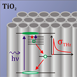 | C Wehrenfennig, CM Palumbiny, HJ Snaith, MB Johnston, L Schmidt-mende, LM Herz
J. Phys. Chem. C, 119:9159-9168 (Apr 2015)
[
pdf ][ SI ][ ref ]
One-dimensional semiconductors such as nanowires and nanotubes are attractive materials for incorporation in photovoltaic devices as they potentially offer short percolation pathways to charge-collecting contacts. We report the observation of free-electron lifetimes in TiO2 nanotubes of the order of tens of picoseconds. These lifetimes are surprisingly short compared to those determined in films of TiO2 nanoparticles. Samples of ordered nanotube arrays with several different tube wall thicknesses were fabricated by anodization and have been investigated by means of optical-pump-terahertz-probe (OPTP) spectroscopy, which allows measurement of transient photoinduced conductivity with picosecond resolution. Our results indicate a two-stage decay of the photoexcited electron population. We attribute the faster component to temporary immobilization of charge in shallow trap states, from which electrons can detrap again by thermal excitation. The slower component most likely reflects irreversible trapping in states deeper below the conduction band edge. Free-electron lifetimes associated with shallow trapping appear to be independent of the tube wall thickness and have very similar values for electrons directly photoexcited in the material and for those injected from an attached photoexcited dye. These results suggest that trap states are not predominantly located at the surface of the tubes. The effective THz charge-carrier mobility in the TiO2 nanotubes is determined (0.1-0.4 cm(2)/(Vs)) and found to be within the same range as carrier mobilities reported for TiO2 nanoparticles. Implications for the relative performance of these nanostructures in dye-sensitized solar cells are discussed.
Citations: 56 (Scopus) 56 (Web of Science) |
- Highly efficient perovskite solar cells with tunable structural color
-
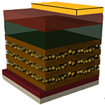 | W Zhang, M Anaya, G Lozano, ME Calvo, MB Johnston, H Miguez, HJ Snaith
Nano Lett., 15:1698-1702 (Mar 2015)
[
pdf ][ SI ][ ref ]
The performance of perovskite solar cells has been progressing over the past few years and efficiency is likely to continue to increase. However, a negative aspect for the integration of perovskite solar cells in the built environment is that the color gamut available in these materials is very limited and does not cover the green-to-blue region of the visible spectrum, which has been a big selling point for organic photovoltaics. Here, we integrate a porous photonic crystal (PC) scaffold within the photoactive layer of an opaque perovskite solar cell following a bottom-up approach employing inexpensive and scalable liquid processing techniques. The photovoltaic devices presented herein show high efficiency with tunable color across the visible spectrum. This now imbues the perovskite solar cells with highly desirable properties for cladding in the built environment and encourages design of sustainable colorful buildings and iridescent electric vehicles as future power generation sources.
Citations: 318 (Scopus) 302 (Web of Science) |
- Single Nanowire Photoconductive Terahertz Detectors
-
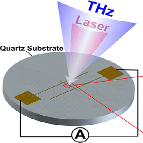 | K Peng, P Parkinson, L Fu, Q Gao, N Jiang, Y Guo, F Wang, HJ Joyce, JL Boland, HH Tan, C Jagadish, MB Johnston
Nano Lett., 15:206-210 (Jan 2015)
[
pdf ][ SI ][ ref ]
Spectroscopy and imaging in the terahertz (THz) region of the electromagnetic spectrum has proven to provide important insights in fields as diverse as chemical analysis, materials characterization, security screening, and nondestructive testing. However, compact optoelectronics suited to the most powerful terahertz technique, time-domain spectroscopy, are lacking. Here, we implement single GaAs nanowires as microscopic coherent THz sensors and for the first time incorporated them into the pulsed time-domain technique. We also demonstrate the functionality of the single nanowire THz detector as a spectrometer by using it to measure the transmission spectrum of a 290 GHz low pass filter. Thus, nanowires are shown to be well suited for THz device applications and hold particular promise as near-field THz sensors.
Citations: 120 (Scopus) 106 (Web of Science) |
- Optical description of mesostructured organic-inorganic halide perovskite solar cells
-
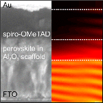 | M Anaya, G Lozano, ME Calvo, W Zhang, MB Johnston, HJ Snaith, H Miguez
J. Phys. Chem. Lett., 6:48-53 (Jan 2015)
[
pdf ][ SI ][ ref ]
Herein we describe both theoretically and experimentally the optical response of solution-processed organic inorganic halide perovskite solar cells based on mesostructured scaffolds. We develop a rigorous theoretical model using a method based on the propagation of waves in layered media, which allows visualizing the way in which light is spatially distributed across the device and serves to quantify the fraction of light absorbed by each medium comprising the cell. The discrimination between productive and parasitic absorption yields an accurate determination of the internal quantum efficiency. State-of-the-art devices integrating mesoporous scaffolds infiltrated with perovskite are manufactured and characterized to support the calculations. This combined experimental and theoretical analysis provides a rational understanding of the optical behavior of perovskite cells and can be beneficial for the judicious design of devices with improved performance. Notably, our model justifies the presence of a solid perovskite capping layer in all of the highest efficiency perovskite solar cells based on thinner mesoporous scaffolds.
Citations: 63 (Scopus) 59 (Web of Science) |
- Efficient, semitransparent neutral-colored solar cells based on microstructured formamidinium lead trihalide perovskite
-
 | GE Eperon, D Bryant, J Troughton, SD Stranks, MB Johnston, T Watson, DA Worsley, HJ Snaith
J. Phys. Chem. Lett., 6:129-138 (Jan 2015)
[
pdf ][ SI ][ ref ]
Efficient, neutral-colored semitransparent solar cells are of commercial interest for incorporation into the windows and surfaces of buildings and automobiles. Here, we report on semitransparent perovskite solar cells that are both efficient and neutral-colored, even in full working devices. Using the microstructured architecture previously developed, we achieve higher efficiencies by replacing methylammonium lead iodide perovskite with formamidinium lead iodide. Current voltage hysteresis is also much reduced. Furthermore, we apply a novel transparent cathode to the devices, enabling us to fabricate neutral-colored semitransparent full solar cells for the first time. Such devices demonstrate over 5% power conversion efficiency for average visible transparencies of almost 30%, retaining impressive color-neutrality. This makes these devices the best-performing single-junction neutral-colored semitransparent solar cells to date. These microstructured perovskite solar cells are shown to have a significant advantage over silicon solar cells in terms of performance at high incident angles of sunlight, making them ideal for building integration.
Citations: 188 (Scopus) 180 (Web of Science) |
- Modulation Doping of GaAs/AlGaAs Core--Shell Nanowires With Effective Defect Passivation and High Electron Mobility
-
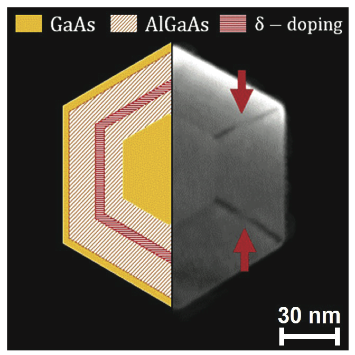 | JL Boland, S Conesa-Boj, P Parkinson, G Tutuncuoglu, F Matteini, D Ruffer, A Casadei, F Amaduzzi, F Jabeen, CL Davies, HJ Joyce, LM Herz, A Fontcuberta i Morral, MB Johnston
Nano Lett., 15:1336-1342 (Jan 2015)
[
pdf ][ SI ][ ref ]
Reliable doping is required to realize many devices based on semiconductor nanowires. Group III–V nanowires show great promise as elements of high-speed optoelectronic devices, but for such applications it is important that the electron mobility is not compromised by the inclusion of dopants. Here we show that GaAs nanowires can be n-type doped with negligible loss of electron mobility. Molecular beam epitaxy was used to fabricate modulation-doped GaAs nanowires with Al0.33Ga0.67As shells that contained a layer of Si dopants. We identify the presence of the doped layer from a high-angle annular dark field scanning electron microscopy cross-section image. The doping density, carrier mobility, and charge carrier lifetimes of these n-type nanowires and nominally undoped reference samples were determined using the noncontact method of optical pump terahertz probe spectroscopy. An n-type extrinsic carrier concentration of 1.10 +- 0.06 × 1016 cm–3 was extracted, demonstrating the effectiveness of modulation doping in GaAs nanowires. The room-temperature electron mobility was also found to be high at 2200 +- 300 cm2 V–1 s–1 and importantly minimal degradation was observed compared with undoped reference nanowires at similar electron densities. In addition, modulation doping significantly enhanced the room-temperature photoconductivity and photoluminescence lifetimes to 3.9 +- 0.3 and 2.4 +- 0.1 ns respectively, revealing that modulation doping can passivate interfacial trap states.
Citations: 83 (Scopus) 79 (Web of Science) |
- Optical properties and limiting photocurrent of thin-film perovskite solar cells
-
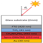 | JM Ball, SD Stranks, MT Horantner, S Huttner, W Zhang, EJW Crossland, I Ramirez, M Riede, MB Johnston, RH Friend, HJ Snaith
Energy Environ. Sci., 8:602-609 ( 2015)
[
pdf ][ SI ][ ref ]
Metal-halide perovskite light-absorbers have risen to the forefront of photovoltaics research offering the potential to combine low-cost fabrication with high power-conversion efficiency. Much of the development has been driven by empirical optimisation strategies to fully exploit the favourable electronic properties of the absorber layer. To build on this progress a full understanding of the device operation requires a thorough optical analysis of the device stack providing a platform for maximising the power conversion efficiency through a precise determination of parasitic losses caused by coherence and absorption in the non-photoactive layers. Here we use an optical model based on the transfer-matrix formalism for analysis of perovskite-based planar heterojunction solar cells using experimentally determined complex refractive index data. We compare the modelled properties to experimentally determined data and obtain good agreement revealing that the internal quantum efficiency in the solar cells approaches 100percent. The modelled and experimental dependence of the photocurrent on incidence angle exhibits only a weak variation{,} with very low reflectivity losses at all angles highlighting the potential for useful power generation over a full daylight cycle.
Citations: 486 (Scopus) 456 (Web of Science) |
- Ultrafast Transient Terahertz Conductivity of Monolayer {MoS$_2$} and {WSe$_2$} Grown by Chemical Vapor Deposition
-
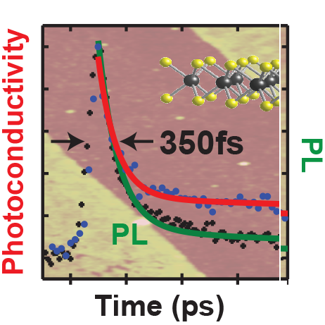 | CJ Docherty, P Parkinson, HJ Joyce, M Chiu, C Chen, M Lee, L Li, LM Herz, MB Johnston
ACS Nano, 8:11147-11153 (Nov 2014)
[
pdf ][ SI ][ ref ]
We have measured ultrafast charge carrier dynamics in monolayers and trilayers of the transition metal dichalcogenides MoS2 and WSe2 using a combination of time-resolved photoluminescence and terahertz spectroscopy. We recorded a photoconductivity and photoluminescence response time of just 350 fs from CVD-grown monolayer MoS2, and 1 ps from trilayer MoS2 and monolayer WSe2. Our results indicate the potential of these materials as high-speed optoelectronic materials.
Citations: 212 (Scopus) 204 (Web of Science) |
- Solution deposition-conversion for planar heterojunction mixed halide perovskite solar cells
-
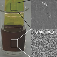 | P Docampo, FC Hanusch, SD Stranks, M Doblinger, JM Feckl, M Ehrensperger, NK Minar, MB Johnston, HJ Snaith, T Bein
Adv. Energy Mater., 4:1400355 (Oct 2014)
[
pdf ][ SI ][ ref ]
The alkylammonium metal trihalide perovskite absorbers first used in working photovoltaic devices were based on liquid elec- trolyte sensitized solar cells. Introduced by Kojima et al., the devices exhibited a starting point power conversion efficiency of 3.8% and, with further work, they were quickly improved to reach over 6%.[1] It was not until a solid-state configuration was employed, however, that high device efficiencies were achieved.[2] Initial results were reported at 9% for perovskite sensitized titania-based devices[2b] and further improvements were simultaneously achieved in a “meso-superstructured” configuration by replacing the mesoporous TiO2 scaffold with an electronically inactive mesoporous Al2O3 layer, exhibiting device efficiencies of over 12%.[2c,3] Some of the key advantages for this material system over other competing device concepts are that they are compatible with solution-processing tech- niques and can be fully processed at low temperatures, thus enabling their use in flexible device applications.[4]
Citations: 330 (Scopus) 328 (Web of Science) |
- Electron Mobilities Approaching Bulk Limits in ``Surface-Free'' {GaAs} Nanowires
-
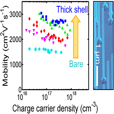 | HJ Joyce, P Parkinson, N Jiang, CJ Docherty, Q Gao, HH Tan, C Jagadish, LM Herz, MB Johnston
Nano Lett., 14:5989-5994 (Sep 2014)
[
pdf ][ SI ][ ref ]
Achieving bulk-like charge carrier mobilities in semiconductor nanowires is a major challenge facing the development of nanowire-based electronic devices. Here we demonstrate that engineering the GaAs nanowire surface by overcoating with optimized AlGaAs shells is an effective means of obtaining exceptionally high carrier mobilities and lifetimes. We performed measurements of GaAs/AlGaAs core–shell nanowires using optical pump-terahertz probe spectroscopy: a noncontact and accurate probe of carrier transport on ultrafast time scales. The carrier lifetimes and mobilities both improved significantly with increasing AlGaAs shell thickness. Remarkably, optimized GaAs/AlGaAs core–shell nanowires exhibited electron mobilities up to 3000 cm2 V–1 s–1, reaching over 65% of the electron mobility typical of high quality undoped bulk GaAs at equivalent photoexcited carrier densities. This points to the high interface quality and the very low levels of ionized impurities and lattice defects in these nanowires. The improvements in mobility were concomitant with drastic improvements in photoconductivity lifetime, reaching 1.6 ns. Comparison of photoconductivity and photoluminescence dynamics indicates that midgap GaAs surface states, and consequently surface band-bending and depletion, are effectively eliminated in these high quality heterostructures.
Citations: 84 (Scopus) 83 (Web of Science) |
- Charge carrier recombination channels in the low-temperature phase of organic-inorganic lead halide perovskite thin films
-
 | C Wehrenfennig, M. Liu, HJ Snaith, MB Johnston, LM Herz
APL Mater., 2:081513 (Aug 2014)
[
pdf ][ SI ][ ref ]
The optoelectronic properties of the mixed hybrid lead halide perovskite CH3NH3PbI3−xClx have been subject to numerous recent studies related to its extraordinary capabilities as an absorber material in thin film solar cells. While the greatest part of the current research concentrates on the behavior of the perovskite at room temperature, the observed influence of phonon-coupling and excitonic effects on charge carrier dynamics suggests that low-temperature phenomena can give valuable additional insights into the underlying physics. Here, we present a temperature-dependent study of optical absorption and photoluminescence (PL) emission of vapor-deposited CH3NH3PbI3−xClx exploring the nature of recombination channels in the room- and the low-temperature phase of the material. On cooling, we identify an up-shift of the absorption onset by about 0.1 eV at about 100 K, which is likely to correspond to the known tetragonal-to-orthorhombic transition of the pure halide CH3NH3PbI3. With further decreasing temperature, a second PL emission peak emerges in addition to the peak from the room-temperature phase. The transition on heating is found to occur at about 140 K, i.e., revealing significant hysteresis in the system. While PL decay lifetimes are found to be independent of temperature above the transition, significantly accelerated recombination is observed in the low-temperature phase. Our data suggest that small inclusions of domains adopting the room-temperature phase are responsible for this behavior rather than a spontaneous increase in the intrinsic rate constants. These observations show that even sparse lower-energy sites can have a strong impact on material performance, acting as charge recombination centres that may detrimentally affect photovoltaic performance but that may also prove useful for optoelectronic applications such as lasing by enhancing population inversion.
Citations: 218 (Scopus) 207 (Web of Science) |
- Charge-carrier dynamics in vapour-deposited films of the organolead halide perovskite {CH$_3$NH$_3$PbI$_{3-x}$Cl$_x$}
-
 | C Wehrenfennig, M. Liu, HJ Snaith, MB Johnston, LM Herz
Energy Environ. Sci., 7:2269--2275 (Jun 2014)
[
pdf ][ SI ][ ref ]
We determine high charge-carrier mobilities [greater-than-or-equal] 33 cm2 V-1 s-1 and bi-molecular recombination rates about five orders of magnitude below the prediction of Langevin{'}s model for vapour-deposited CH3NH3PbI3-xClx using ultrafast THz spectroscopy. At charge-carrier densities below [similar]1017 cm-3 intrinsic diffusion lengths are shown to approach 3 microns{,} limited by slow mono-molecular decay processes.}
Citations: 467 (Scopus) 453 (Web of Science) |
- An ultrafast carbon nanotube terahertz polarisation modulator
-
 | CJ Docherty, SD Stranks, SN Habisreutinger, HJ Joyce, LM Herz, RJ Nicholas, MB Johnston
J. Appl. Phys., 115:203108 (May 2014)
[
pdf ][ SI ][ ref ]
We demonstrate ultrafast modulation of terahertz radiation by unaligned optically pumped single-walled carbon nanotubes. Photoexcitation by an ultrafast optical pump pulse induces transient terahertz absorption in nanowires aligned parallel to the optical pump. By controlling the polarisation of the optical pump, we show that terahertz polarisation and modulation can be tuned, allowing sub-picosecond modulation of terahertz radiation. Such speeds suggest potential for semiconductor nanowire devices in terahertz communication technologies.
Citations: 38 (Scopus) 37 (Web of Science) |
- Homogeneous Emission Line Broadening in the Organo Lead Halide Perovskite $CH_3NH_3PbI_{3-x}Cl_x$
-
 | C Wehrenfennig, M. Liu, HJ Snaith, MB Johnston, LM Herz
J. Phys. Chem. Lett., 5:1300-1306 (Apr 2014)
[
pdf ][ SI ][ ref ]
The organic−inorganic hybrid perovskites methylammonium lead iodide (CH3NH3PbI3) and the partially chlorine-substituted mixed halide CH3NH3PbI3−xClx emit strong and broad photoluminescence (PL) around their band gap energy of ∼1.6 eV. However, the nature of the radiative decay channels behind the observed emission and, in particular, the spectral broadening mechanisms are still unclear. Here we investigate these processes for high-quality vapor-deposited films of CH3NH3PbI3−xClx using time- and excitation-energy dependent photoluminescence spectroscopy. We show that the PL spectrum is homogenously broadened with a line width of 103 meV most likely as a consequence of phonon coupling effects. Further analysis reveals that defects or trap states play a minor role in radiative decay channels. In terms of possible lasing applications, the emission spectrum of the perovskite is sufficiently broad to have potential for amplification of light pulses below 100 fs pulse duration.
Citations: 353 (Scopus) 344 (Web of Science) |
- High Charge Carrier Mobilities and Lifetimes in Organolead Trihalide Perovskites
-
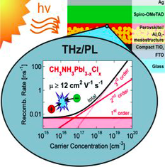 | C Wehrenfennig, GE Eperon, MB Johnston, HJ Snaith, LM Herz
Adv. Mater., 26:1584-1589 (Mar 2014)
[
pdf ][ SI ][ ref ]
Organolead trihalide perovskites are shown to exhibit the best of both worlds: charge carrier mobilities around 10 cm2/V/s and low bi-molecular charge recombination constants. The ratio of the two is found to defy the Langevin limit of kinetic charge capture by over four orders of magnitude. This mechanism causes long (micron) charge-pair diffusion lengths crucial for flat-heterojunction photovoltaics.
Citations: 3068 (Scopus) 2965 (Web of Science) |
- Formamidinium lead trihalide: a broadly tunable perovskite for efficient planar heterojunction solar cells
-
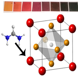 | GE Eperon, SD Stranks, C Menelaou, MB Johnston, LM Herz, HJ Snaith
Energy Environ. Sci., 7:982-988 (Mar 2014)
[
pdf ][ SI ][ ref ]
Perovskite-based solar cells have attracted significant recent interest, with power conversion efficiencies in excess of 15% already superceding a number of established thin-film solar cell technologies. Most work has focused on a methylammonium lead trihalide perovskites, with a bandgaps of ~1.55 eV and greater. Here, we explore the effect of replacing the methylammonium cation in this perovskite, and show that with the slightly larger formamidinium cation, we can synthesise formamidinium lead trihalide perovskites with a bandgap tunable between 1.48 and 2.23 eV. We take the 1.48 eV-bandgap perovskite as most suited for single junction solar cells, and demonstrate long-range electron and hole diffusion lengths in this material, making it suitable for planar heterojunction solar cells. We fabricate such devices, and due to the reduced bandgap we achieve high short-circuit currents of >23 mA cm-2, resulting in power conversion efficiencies of up to 14.2%, the highest efficiency yet for solution processed planar heterojunction perovskite solar cells. Formamidinium lead triiodide is hence promising as a new candidate for this class of solar cell.
Citations: 3851 (Scopus) 3691 (Web of Science) |
- Dependence of Dye Regeneration and Charge Collection on the Pore-Filling Fraction in Solid-State Dye-Sensitized Solar Cells
-
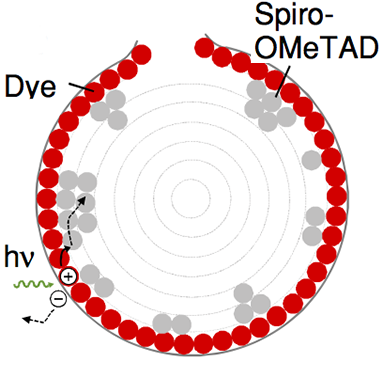 | CT Weisspfennig, DJ Hollman, C Menelaou, SD Stranks, HJ Joyce, MB Johnston, HJ Snaith, LM Herz
Adv. Funct. Mater., 24:668--677 (Feb 2014)
[
pdf ][ SI ][ ref ]
Solid-state dye-sensitized solar cells rely on effective infiltration of a solid-state hole-transporting material into the pores of a nanoporous TiO2 network to allow for dye regeneration and hole extraction. Using microsecond transient absorption spectroscopy and femtosecond photoluminescence upconversion spectroscopy, the hole-transfer yield from the dye to the hole-transporting material 2,2′,7,7′-tetrakis(N,N-di-p-methoxyphenylamine)-9,9'-spirobifluorene (spiro-OMeTAD) is shown to rise rapidly with higher pore-filling fractions as the dye-coated pore surface is increasingly covered with hole-transporting material. Once a pore-filling fraction of ≈30% is reached, further increases do not significantly change the hole-transfer yield. Using simple models of infiltration of spiro-OMeTAD into the TiO2 porous network, it is shown that this pore-filling fraction is less than the amount required to cover the dye surface with at least a single layer of hole-transporting material, suggesting that charge diffusion through the dye monolayer network precedes transfer to the hole-transporting material. Comparison of these results with device parameters shows that improvements of the power-conversion efficiency beyond ≈30% pore filling are not caused by a higher hole-transfer yield, but by a higher charge-collection efficiency, which is found to occur in steps. The observed sharp onsets in photocurrent and power-conversion efficiencies with increasing pore-filling fraction correlate well with percolation theory, predicting the points of cohesive pathway formation in successive spiro-OMeTAD layers adhered to the pore walls. From percolation theory it is predicted that, for standard mesoporous TiO2 with 20 nm pore size, the photocurrent should show no further improvement beyond an ≈83% pore-filling fraction.
Citations: 34 (Scopus) 32 (Web of Science) |
- Single GaAs/AlGaAs Nanowire Photoconductive
Terahertz Detectors
-
 | K Peng, P Parkinson, L Fu, Q Gao, N Jiang, Y Guo, F Wang, HJ Joyce, JL Boland, MB Johnston, HH Tan, C Jagadish
, 2014:221-222 ( 2014)
[
pdf ][ SI ][ ref ]
Photoconductive terahertz detectors based on single GaAs/AlGaAs core-shell nanowire have been designed and fabricated. The devices were characterised in a terahertz time-domain spectroscopy system, showing excellent sensitivity comparable to the standard bulk ion-implanted InP receiver, with a detection bandwidth of 0.1 ~ 0.6 THz. Finite-difference time-domain simulations were performed to understand the origin of the narrow bandwidth of current detectors as well as optimize antenna designs to improve detector performance.
|
- Direct Observation of Charge-Carrier Heating at WZ--ZB {InP} Nanowire Heterojunctions
-
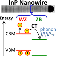 | CK Yong, J Wong-Leung, HJ Joyce, J Lloyd-Hughes, Q Gao, HH Tan, C Jagadish, MB Johnston, LM Herz
Nano Lett., 13:4280-4287 (Sep 2013)
[
pdf ][ SI ][ ref ]
We have investigated the dynamics of hot charge carriers in InP nanowire ensembles containing a range of densities of zinc-blende inclusions along the otherwise wurtzite nanowires. From time-dependent photoluminescence spectra, we extract the temperature of the charge carriers as a function of time after nonresonant excitation. We find that charge-carrier temperature initially decreases rapidly with time in accordance with efficient heat transfer to lattice vibrations. However, cooling rates are subsequently slowed and are significantly lower for nanowires containing a higher density of stacking faults. We conclude that the transfer of charges across the type II interface is followed by release of additional energy to the lattice, which raises the phonon bath temperature above equilibrium and impedes the carrier cooling occurring through interaction with such phonons. These results demonstrate that type II heterointerfaces in semiconductor nanowires can sustain a hot charge-carrier distribution over an extended time period. In photovoltaic applications, such heterointerfaces may hence both reduce recombination rates and limit energy losses by allowing hot-carrier harvesting.
Citations: 35 (Scopus) 36 (Web of Science) |
- Efficient planar heterojunction perovskite solar cells by vapour deposition
-
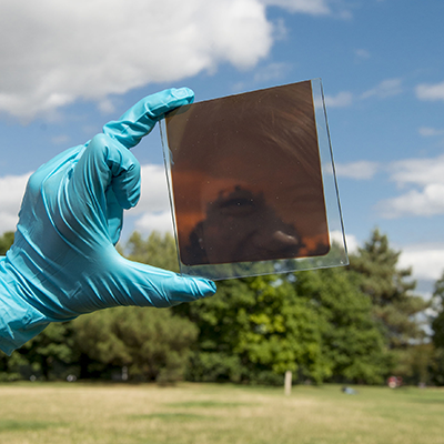 | M. Liu, MB Johnston, HJ Snaith
Nature, 501:395--398 (Sep 2013)
[
pdf ][ SI ][ ref ]
Many different photovoltaic technologies are being developed for large-scale solar energy conversion1, 2, 3, 4. The wafer-based first-generation photovoltaic devices1 have been followed by thin-film solid semiconductor absorber layers sandwiched between two charge-selective contacts3 and nanostructured (or mesostructured) solar cells that rely on a distributed heterojunction to generate charge and to transport positive and negative charges in spatially separated phases4, 5, 6. Although many materials have been used in nanostructured devices, the goal of attaining high-efficiency thin-film solar cells in such a way has yet to be achieved7. Organometal halide perovskites have recently emerged as a promising material for high-efficiency nanostructured devices8, 9, 10, 11. Here we show that nanostructuring is not necessary to achieve high efficiencies with this material: a simple planar heterojunction solar cell incorporating vapour-deposited perovskite as the absorbing layer can have solar-to-electrical power conversion efficiencies of over 15 per cent (as measured under simulated full sunlight). This demonstrates that perovskite absorbers can function at the highest efficiencies in simplified device architectures, without the need for complex nanostructures.
Citations: 7611 (Scopus) 7238 (Web of Science) |
- Electronic properties of {GaAs}, {InAs} and {InP} nanowires studied by terahertz spectroscopy
-
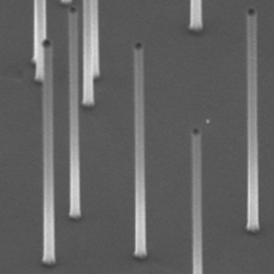 | HJ Joyce, CJ Docherty, Q Gao, HH Tan, C Jagadish, J Lloyd-Hughes, LM Herz, MB Johnston
Nanotechnology, 24:214006 (May 2013)
[
pdf ][ SI ][ ref ]
We have performed a comparative study of ultrafast charge carrier dynamics in a range of III–V nanowires using optical pump–terahertz probe spectroscopy. This versatile technique allows measurement of important parameters for device applications, including carrier lifetimes, surface recombination velocities, carrier mobilities and donor doping levels. GaAs, InAs and InP nanowires of varying diameters were measured. For all samples, the electronic response was dominated by a pronounced surface plasmon mode. Of the three nanowire materials, InAs nanowires exhibited the highest electron mobilities of 6000 cm^2/V/s , which highlights their potential for high mobility applications, such as field effect transistors. InP nanowires exhibited the longest carrier lifetimes and the lowest surface recombination velocity of 170 cm/s. This very low surface recombination velocity makes InP nanowires suitable for applications where carrier lifetime is crucial, such as in photovoltaics. In contrast, the carrier lifetimes in GaAs nanowires were extremely short, of the order of picoseconds, due to the high surface recombination velocity, which was measured as 5.4 × 10^5 cm/s. These findings will assist in the choice of nanowires for different applications, and identify the challenges in producing nanowires suitable for future electronic and optoelectronic devices.
Citations: 291 (Scopus) 261 (Web of Science) |
- Optimizing the Energy Offset between Dye and Hole-Transporting Material in Solid-State Dye-Sensitized Solar Cells
-
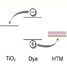 | CT Weisspfennig, MM Lee, J Teuscher, P Docampo, SD Stranks, HJ Joyce, H Bergmann, I Bruder, DV Kondratuk, MB Johnston, HJ Snaith, LM Herz
J. Phys. Chem. C, 117:19850-19858 ( 2013)
[
pdf ][ SI ][ ref ]
The power-conversion efficiency of solid-state dye-sensitized solar cells can be optimized by reducing the energy offset between the highest occupied molecular orbital (HOMO) levels of dye and hole-transporting material (HTM) to minimize the loss-in-potential. Here, we report a study of three novel HTMs with HOMO levels slightly above and below the one of the commonly used HTM 2,2′,7,7′- tetrakis(N,N-di-p-methoxyphenylamino)-9,9′-spirobifluorene (spiro-OMeTAD) to systematically explore this possibility. Using transient absorption spectroscopy and employing the ruthenium based dye Z907 as sensitizer, it is shown that, despite one new HTM showing a 100% hole-transfer yield, all devices based on the new HTMs performed worse than those incorporating spiro-OMeTAD. We further demonstrate that the design of the HTM has an additional impact on the electronic density of states present at the TiO2 electrode surface and hence influences not only hole- but also electron-transfer from the sensitizer. These results provide insight into the complex influence of the HTM on charge transfer and provide guidance for the molecular design of new materials.
Citations: 20 (Scopus) 20 (Web of Science) |
- Strong Carrier Lifetime Enhancement in {GaAs} Nanowires Coated with Semiconducting Polymer
-
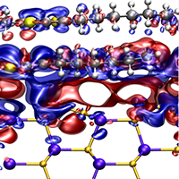 | CK Yong, K Noori, Q Gao, HJ Joyce, HH Tan, C Jagadish, F Giustino, MB Johnston, LM Herz
Nano Lett., 12:6293-6301 (Dec 2012)
[
pdf ][ SI ][ ref ]
The ultrafast charge carrier dynamics in GaAs/conjugated polymer type II heterojunctions are investigated using time-resolved photoluminescence spectroscopy at 10 K. By probing the photoluminescence at the band edge of GaAs, we observe strong carrier lifetime enhancement for nanowires blended with semiconducting polymers. The enhancement is found to depend crucially on the ionization potential of the polymers with respect to the Fermi energy level at the surface of the GaAs nanowires. We attribute these effects to electron doping by the polymer which reduces the unsaturated surface-state density in GaAs. We find that when the surface of nanowires is terminated by native oxide, the electron injection across the interface is greatly reduced and such surface doping is absent. Our results suggest that surface engineering via π-conjugated polymers can substantially improve the carrier lifetime in nanowire hybrid heterojunctions with applications in photovoltaics and nanoscale photodetectors.
Citations: 62 (Scopus) 62 (Web of Science) |
- Extreme sensitivity of graphene photoconductivity to environmental gases
-
 | CJ Docherty, C Lin, HJ Joyce, RJ Nicholas, LM Herz, L Li, MB Johnston
Nat. Commun., 3:1228 (Nov 2012)
[
pdf ][ SI ][ ref ]
Graphene is a single layer of covalently bonded carbon atoms, which was discovered only 8 years ago and yet has already attracted intense research and commercial interest. Initial research focused on its remarkable electronic properties, such as the observation of massless Dirac fermions and the half-integer quantum Hall effect. Now graphene is finding application in touch-screen displays, as channels in high-frequency transistors and in graphene-based integrated circuits. The potential for using the unique properties of graphene in terahertz-frequency electronics is particularly exciting; however, initial experiments probing the terahertz-frequency response of graphene are only just emerging. Here we show that the photoconductivity of graphene at terahertz frequencies is dramatically altered by the adsorption of atmospheric gases, such as nitrogen and oxygen. Furthermore, we observe the signature of terahertz stimulated emission from gas-adsorbed graphene. Our findings highlight the importance of environmental conditions on the design and fabrication of high-speed, graphene-based devices.
Citations: 143 (Scopus) 138 (Web of Science) |
- Ultra-low Surface Recombination Velocity in InP Nanowires Probed by Terahertz Spectroscopy
-
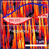 | HJ Joyce, J Wong-Leung, C Yong, CJ Docherty, S Paiman, Q Gao, HH Tan, C Jagadish, J Lloyd-Hughes, LM Herz, MB Johnston
Nano Lett., 12:5325-5330 (Oct 2012)
[
pdf ][ SI ][ ref ]
Using transient terahertz photoconductivity measurements, we have made non-contact, room temperature measurements of the ultrafast charge carrier dynamics in InP nanowires. InP nanowires exhibited a very long photoconductivity lifetime of over 1ns, and carrier lifetimes were remarkably insensitive to surface states despite the large nanowire surface area-to-volume ratio. An exceptionally low surface recombination velocity (170cm/s) was recorded at room temperature. These results suggest that InP nanowires are prime candidates for optoelectronic devices, particularly photovoltaic devices, without the need for surface passivation. We found that the carrier mobility is not limited by nanowire diameter, but is strongly limited by the presence of planar crystallographic defects such as stacking faults in these predominantly wurtzite nanowires. These findings show the great potential of very narrow InP nanowires for electronic devices, but indicate that improvements in the crystallographic uniformity of InP nanowires will be critical for future nanowire device engineering.
Citations: 171 (Scopus) 163 (Web of Science) |
- Noncontact Measurement of Charge Carrier Lifetime and Mobility in {GaN} Nanowires
-
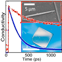 | P Parkinson, C Dodson, HJ Joyce, KA Bertness, NA Sanford, LM Herz, MB Johnston
Nano Lett., 12:4600--4604 (Sep 2012)
[
pdf ][ SI ][ ref ]
The first noncontact photoconductivity measurements of gallium nitride nanowires (NWs) are presented, revealing a high crystallographic and optoelectronic quality achieved by use of catalyst-free molecular beam epitaxy. In comparison with bulk material, the NWs exhibit a long conductivity lifetime (>2 ns) and a high mobility (820 ± 120 cm2/(V s)). This is due to the weak influence of surface traps with respect to other III–V semiconducting NWs and to the favorable crystalline structure of the NWs achieved via strain-relieved growth.
Citations: 71 (Scopus) 65 (Web of Science) |
- Simulation of fluence-dependent photocurrent in terahertz photoconductive receivers
-
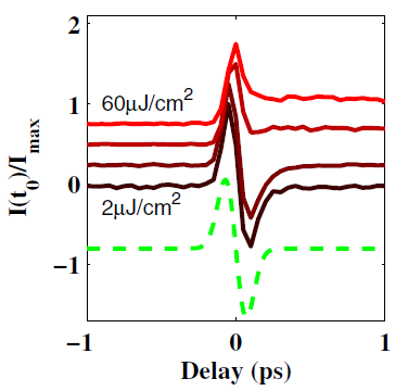 | E Castro-Camus, MB Johnston, J Lloyd-Hughes
Semicond. Sci. Technol., 27:115011 (Sep 2012)
[
pdf ][ SI ][ ref ]
A semi-classical Monte Carlo simulation of carrier dynamics in photoconductive detectors of terahertz (THz) radiation is presented. We have used this simulation to elucidate the importance of carrier trapping in the operation of photoconductive detectors. Simulations of the detection of single-cycle THz pulses by photoconductive antennas based on GaAs with trap densities between 2 × 10 17 and 2 × 10 18 cm −3 are presented. We show that the high frequency (>1 THz) spectral response of photoconductive devices decreases with increasing excitation fluence. Our simulations reveal that this effect is a direct consequence of the saturation of trapping centres.
Citations: 16 (Scopus) 14 (Web of Science) |
- Nanoengineering Coaxial Carbon Nanotube--Dual-Polymer Heterostructures
-
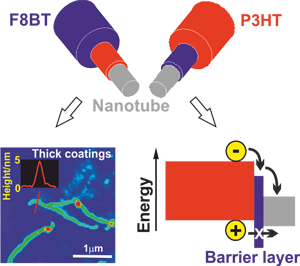 | SD Stranks, C Yong, JA Alexander-Webber, C Weisspfennig, MB Johnston, LM Herz, RJ Nicholas
ACS Nano, 6:6058--6066 (Jul 2012)
[
pdf ][ SI ][ ref ]
We describe studies of new nanostructured materials consisting of carbon nanotubes wrapped in sequential coatings of two different semiconducting polymers, namely, poly(3- hexylthiophene) (P3HT) and poly(9,90-dioctylfluorene-co-benzothiadiazole) (F8BT). Using absorption spectroscopy and steady-state and ultrafast photoluminescence measurements, we demonstrate the role of the different layer structures in controlling energy levels and charge transfer in both solution and film samples. By varying the simple solution processing steps, we can control the ordering and proportions of the wrapping polymers in the solid state. The resulting novel coaxial structures open up a variety of new applications for nanotube blends and are particularly promising for implementation into organic photovoltaic devices. The carbon nanotube template can also be used to optimize both the electronic properties and morphology of polymer composites in a much more controlled fashion than achieved previously, offering a route to producing a new generation of polymer nanostructures.
Citations: 39 (Scopus) 38 (Web of Science) |
- Terahertz properties of graphene
-
 | CJ Docherty, MB Johnston
J Infrared Milli Terahz Waves, 33:797 (Jul 2012)
[
pdf ][ SI ][ ref ]
Graphene has proved itself as being unique in terms of fundamental physics, and of particular importance for post–silicon electronics. Research into graphene has divided into two branches, one probing the remarkable electronic and optical properties of graphene, and the other pursuing technologically viable forms of the material. Terahertz time domain spectroscopy (THz TDS) is a powerful tool for both, able to characterise the free carrier response of graphene and probe the inter and intraband response of excited carriers with sub-ps time resolution. We review THz TDS and related THz measurements of graphene.
Citations: 97 (Scopus) 81 (Web of Science) |
- Ultrafast Dynamics of Exciton Formation in Semiconductor Nanowires
-
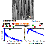 | CK Yong, HJ Joyce, J Lloyd-Hughes, Q Gao, HH Tan, C Jagadish, MB Johnston, LM Herz
Small, 8:1725--1731 (Jun 2012)
[
pdf ][ SI ][ ref ]
The dynamics of free electron–hole pairs and excitons in GaAs–AlGaAs–GaAs core–shell–skin nanowires is investigated using femtosecond transient photoluminescence spectroscopy at 10 K. Following nonresonant excitation, a bimolecular interconversion of the initially generated electron–hole plasma into an exciton population is observed. This conducting-to-insulating transition appears to occur gradually over electron–hole charge pair densities of 2–4 × 10^16 cm-3. The smoothness of the Mott transition is attributed to the slow carrier-cooling during the bimolecular interconversion of free charge carriers into excitons and to the presence of chemical-potential fluctuations leading to inhomogeneous spectral characteristics. These results demonstrate that high-quality nanowires are model systems for investigating fundamental scientific effects in 1D heterostructures.
Citations: 19 (Scopus) 19 (Web of Science) |
- Introduction to the Special Issue on Photoconductive Emission and Detection of Terahertz Radiation
-
 | MB Johnston
J Infrared Milli Terahz Waves, 33:391-392 (Apr 2012)
[
pdf ][ SI ][ ref ]
Terahertz science and technology is a research area that has expanded rapidly in the past
decade, with terahertz spectroscopy and imaging now becoming important tools in applications
as diverse as nanotechnology and industrial quality control. The power of terahertz
spectroscopy is based on the ability to generate coherent terahertz radiation and to detect its
electric field as a function of time. Photoconductive devices were the key technologies that
first enabled such coherent emission and detection, and thus seeded modern terahertz
spectroscopy. Intense research into photoconductive device technology is currently leading
to devices that are highly efficient, robust and industrially compatible. Furthermore, novel
photoconductive devices are stimulating the development of yet more novel forms of
spectroscopy, and new applications. This Special Issue is devoted to assessing the present
status of photoconductive terahertz technologies and to discussing future challenges facing
the field.
|
- The Origin of an Efficiency Improving Light Soaking Effect in SnO$_2$ Based Solid-State Dye-Sensitized Solar Cells
-
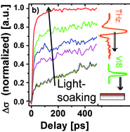 | P Tiwana, P Docampo, MB Johnston, LM Herz, HJ Snaith
Energy Environ. Sci., 5:9566-9573 ( 2012)
[
pdf ][ SI ][ ref ]
We observe a strong light-soaking effect in SnO2 based solid-state dye-sensitized solar cells (SDSCs). Both with and without the presence of UV light, the devices short-circuit photocurrent and efficiency increase significantly over 20-30 minutes, until steady-state is achieved. We demonstrate that this is not due to improved charge collection and investigate the charge generation dynamics employing optical-pump terahertz-probe spectroscopy. We observe a monotonic speeding-up of the generation of free-electrons in the SnO2 conduction band as a function of the light-soaking time. This improved charge generation can be explained by a positive shift in the conduction band edge or, alternatively, an increase in the density of states (DoS) at the energy at which photoinduced electron transfer o
Citations: 71 (Scopus) 68 (Web of Science) |
- Electron Mobility and Injection Dynamics in Mesoporous {ZnO, SnO$_2$, and TiO$_2$} Films Used in Dye-Sensitized Solar Cells
-
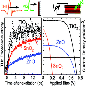 | P Tiwana, P Docampo, MB Johnston, HJ Snaith, LM Herz
ACS Nano, 5:5158-5166 (Jun 2011)
[
pdf ][ SI ][ ref ]
High-performance dye-sensitized solar cells are usually fabricated using nanostructured TiO2 as a thin-film electron-collecting material. However, alternative metal-oxides are currently being explored that may offer advantages through ease of processing, higher electron mobility, or interface band energetics. We present here a comparative study of electron mobility and injection dynamics in thin films of TiO2, ZnO, and SnO2 nanoparticles sensitized with Z907 ruthenium dye. Using time-resolved terahertz photoconductivity measurements, we show that, for ZnO and SnO2 nanoporous films, electron injection from the sensitizer has substantial slow components lasting over tens to hundreds of picoseconds, while for TiO2, the process is predominantly concluded within a few picoseconds. These results correlate well with the overall electron injection efficiencies we determine from photovoltaic cells fabricated from identical nanoporous films, suggesting that such slow components limit the overall photocurrent generated by the solar cell. We conclude that these injection dynamics are not substantially influenced by bulk energy level offsets but rather by the local environment of the dye-nanoparticle interface that is governed by dye binding modes and densities of states available for injection, both of which may vary from site to site. In addition, we have extracted the electron mobility in the three nanoporous metal-oxide films at early time after excitation from terahertz conductivity measurements and compared these with the time-averaged, long-range mobility determined for devices based on identical films. Comparison with established values for single-crystal Hall mobilities of the three materials shows that, while electron mobility values for nanoporous TiO2 films are approaching theoretical maximum values, both early time, short distance and interparticle electron mobility in nanoporous ZnO or SnO2 films offer considerable scope for improvement.
Citations: 772 (Scopus) 734 (Web of Science) |
- {III}--{V} semiconductor nanowires for optoelectronic device applications
-
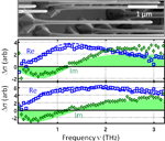 | HJ Joyce, Q Gao, HH Tan, C Jagadish, Y Kim, J Zou, LM Smith, HE Jackson, JM Yarrison-Rice, P Parkinson, MB Johnston
Prog. Quantum Electron., 35:23-75 (Mar 2011)
[
pdf ][ SI ][ ref ]
Semiconductor nanowires have recently emerged as a new class of materials with significant potential to reveal new fundamental physics and to propel new applications in quantum electronic and optoelectronic devices. Semiconductor nanowires show exceptional promise as nanostructured materials for exploring physics in reduced dimensions and in complex geometries, as well as in one-dimensional nanowire devices. They are compatible with existing semiconductor technologies and can be tailored into unique axial and radial heterostructures. In this contribution we review the recent efforts of our international collaboration which have resulted in significant advances in the growth of exceptionally high quality III–V nanowires and nanowire heterostructures, and major developments in understanding the electronic energy landscapes of these nanowires and the dynamics of carriers in these nanowires using photoluminescence, time-resolved photoluminescence and terahertz conductivity spectroscopy.
Citations: 267 (Scopus) 262 (Web of Science) |
- All-optical full-color displays using polymer nanofibers
-
 | HQ Yu, DW Liao, MB Johnston, BJ Li
ACS Nano, 5:2020-2025 (Mar 2011)
[
pdf ][ SI ][ ref ]
We report a number of crossed nanofiber structures for full-color micro/nanodisplays, which were formed by assembling flexible poly(trimethylene terephthalate) (PTT) nanofibers under an optical microscope with the assistance of micromanipulators. The color pixels of the displays consist of micro/nanometer sized color spots in a radius of 300-1500 nm, which were realized through crossed junctions of the PTT nanofibers. The colors of the spots were tuned by changing the power ratios of the launched red, green, and blue lights. We further present a new way to develop white light illumination by combination of red, green, and blue lights with assembly techniques and low production costs.
Citations: 41 (Scopus) 39 (Web of Science) |
- Ultrafast Charge Separation at a Polymer-Single-Walled Carbon Nanotube Molecular Junction
-
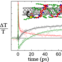 | SD Stranks, C Weisspfennig, P Parkinson, MB Johnston, LM Herz, RJ Nicholas
Nano Lett., 11:66-72 (Jan 2011)
[
pdf ][ SI ][ ref ]
We have investigated the charge photogeneration dynamics at the interface formed between single-walled carbon nanotubes (SWNTs) and poly(3-hexylthiophene) (P3HT) using a combination of femtosecond spectroscopic techniques. We demonstrate that photoexcitation of P3HT forming a single molecular layer around a SWNT leads to an ultrafast (~430 fs) charge transfer between the materials. The addition of excess P3HT leads to long-term charge separation in which free polarons remain separated at room temperature. Our results suggest that SWNT-P3HT blends incorporating only small fractions (1%) of SWNTs allow photon-to-charge conversion with efficiencies comparable to those for conventional (60:40) P3HT−fullerene blends, provided that small-diameter tubes are individually embedded in the P3HT matrix.
Citations: 86 (Scopus) 78 (Web of Science) |
- Improved performance of {GaAs}-based terahertz emitters via surface passivation and silicon nitride encapsulation
-
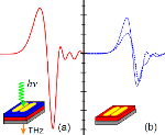 | C Headley, L Fu, P Parkinson, XL Xu, J Lloyd-Hughes, C Jagadish, MB Johnston
IEEE J. Sel. Top. Quantum Electron., 17:17-21 (Jan 2011)
[
pdf ][ SI ][ ref ]
We have improved the stability and performance of terahertz (THz) photoconductive (Auston) switches using a combination of (NH4)(2)S surface passivation (SP) and silicon nitride (Si3N4) encapsulation. The influences of SP and encapsulation on the ultrafast electron dynamics in GaAs were examined using THz emission spectroscopy and optical pump-THz probe spectroscopy. The power of THz radiation from the surface of photoexcited GaAs increased by a factor of 5 after passivation and encapsulation, while the process lengthened the trapping time for photoexcited charge carriers. By fabricating and assessing the performance of photoconductive switches, we found that passivation and encapsulation increased the average THz power generated fourfold.
Citations: 34 (Scopus) 30 (Web of Science) |
- Role of Ultrafast Torsional Relaxation in the Emission from Polythiophene Aggregates
-
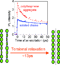 | P Parkinson, C Muller, N Stingelin, MB Johnston, LM Herz
J. Phys. Chem. Lett., 1:2788-2792 (Sep 2010)
[
pdf ][ SI ][ ref ]
An understanding of aggregation effects in semiconducting polymers is essential for their use in optoelectronic devices; however, the dynamic evolution of such interchain states is not well understood. Here, we have investigated a blend of semiconducting poly(3-hexylthiophene) (P3HT) with an electronically inert ultrahigh-molecular-weight polyethylene (UHMW-PE) matrix that is shown to allow precise control over the extent to which the P3HT chains aggregate. We determined the singlet exciton population within isolated and aggregated P3HT regions using femtosecond time-resolved photoluminescence measurements and found a strong ultrafast decay pathway in the aggregated case only. Comparison of the emission from the two lowest vibronic bands demonstrates a changeover from an initial vibrationally “hot” photoexcited state to a geometrically relaxed aggregate state within 13 ps, corresponding to time scales for torsional relaxation in these materials. We conclude that formation of an aggregate excited state in conjugated polymers is mediated by vibrational relaxation from a low-symmetry to a high-symmetry ordered state for the ensemble.
Citations: 94 (Scopus) 93 (Web of Science) |
- Dynamic terahertz polarization in single-walled carbon nanotubes
-
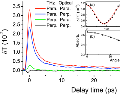 | XL Xu, P Parkinson, K-C Chuang, MB Johnston, RJ Nicholas, LM Herz
Phys. Rev. B, 82:085441 (Aug 2010)
[
pdf ][ SI ][ ref ]
We have investigated the anisotropic dynamic dielectric response of aligned and well-isolated single-walled carbon nanotubes using optical-pump terahertz (THz)-probe techniques. The polarization anisotropy measurements demonstrate that the THz radiation interacts only with radiation polarized parallel to the nanotubes which have been selectively excited by a polarized pump pulse thus allowing controlled THz polarization to be achieved from unaligned nanotubes.
Citations: 28 (Scopus) 25 (Web of Science) |
- Terahertz emission from lateral photo-{Dember} currents
-
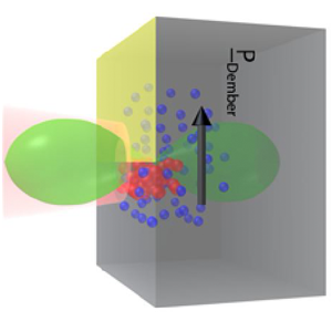 | G Klatt, F Hilser, W Qiao, M Beck, R Gebs, A Bartels, K Huska, U Lemmer, G Bastian, MB Johnston, M Fischer, J Faist, T Dekorsy
Opt. Express, 18:4939-4947 (Mar 2010)
[
pdf ][ SI ][ ref ]
The photo-Dember effect is a source of impulsive THz emission following femtosecond pulsed optical excitation. This emission results from the ultrafast spatial separation of electron-hole pairs in strong carrier gradients due to their different diffusion coefficients. The associated time dependent polarization is oriented perpendicular to the excited surface which is inaptly for efficient out coupling of THz radiation. We propose a scheme for generating strong carrier gradients parallel to the excited surface. The resulting photo-Dember currents are oriented in the same direction and emit THz radiation into the favorable direction perpendicular to the surface. This effect is demonstrated for GaAs and In0.53Ga0.47As. Surprisingly the photo-Dember THz emitters provide higher bandwidth than photoconductive emitters. Multiplexing of phase coherent photo-Dember currents by periodically tailoring the photoexcited spatial carrier distribution gives rise to a strongly enhanced THz emission, which reaches electric field amplitudes comparable to a high-efficiency externally biased photoconductive emitter. (C) 2010 Optical Society of America
Citations: 140 (Scopus) 122 (Web of Science) |
- Ultrafast Terahertz Conductivity Dynamics in Mesoporous {TiO}$_2$: {Influence} of Dye Sensitization and Surface Treatment in Solid-State Dye-Sensitized Solar Cells
-
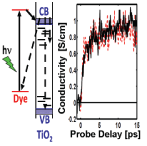 | P Tiwana, P Parkinson, MB Johnston, HJ Snaith, LM Herz
J. Phys. Chem. C, 114:1365-1371 (Jan 2010)
[
pdf ][ SI ][ ref ]
We have used optical-pump terahertz-probe spectroscopy to explore the photoinduced conductivity dynamics in mesoporous anatase TiO2 films, commonly employed as the electron-transporting electrode in dye-sensitized solar cells. We find an intrinsic mobility value of 0.1 cm(2)/(V s) and diffusion length of similar to 20 nm for electron motion through the TiO2 matrix. The photoconductivity dynamics in TiO2 films, both before and after sensitization with a ruthenium bypyridyl complex termed Z907, were examined in order to study the charge injection, trapping, and recombination time scales. We observe a biphasic charge injection from Z907, with a fast sub-500 fs component, followed by a slower 70-200 ps component. This is followed by photoconductivity decay over the first few nanoseconds, predominantly reflecting charge carrier trapping. In addition, we have utilized terahertz spectroscopy to investigate the influence of treating the titania surface with TiCl4 on early-time charge dynamics, In the solar Cells, Surface treatment of the mesoporous TiO2 with TiCl4 is critical to enable efficient operation. Here, we find that neither early-time charge mobility, nor charge injection rate or decay times are significantly affected by the treatment, which suggests that it may instead have an impact on phenomena occurring on longer time scales.
Citations: 85 (Scopus) 82 (Web of Science) |
- Extraction of the anisotropic dielectric properties of materials from polarization-resolved terahertz time-domain spectra
-
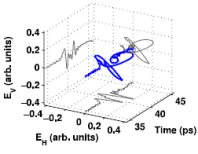 | E Castro-Camus, MB Johnston
J. Opt. A-Pure Appl. Opt., 11:105206 (Oct 2009)
[
pdf ][ SI ][ ref ]
The anisotropic complex dielectric properties of materials in the terahertz band is a topic that has attracted considerable attention recently in the fields of physics, chemistry and biochemistry. The mathematical formalism for analysing polarization-resolved terahertz time-domain data is presented, and particular cases including birefringence, optical activity and circular dichroism are discussed.
Citations: 40 (Scopus) 34 (Web of Science) |
- Carrier lifetime and mobility enhancement in nearly defect-free core--shell nanowires measured using time-resolved terahertz spectroscopy
-
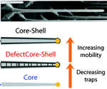 | P Parkinson, HJ Joyce, Q Gao, HH Tan, X Zhang, J Zou, C Jagadish, LM Herz, MB Johnston
Nano Lett., 9:3349-3353 (Sep 2009)
[
pdf ][ SI ][ ref ]
We have used transient terahertz photoconductivity measurements to assess the efficacy of two-temperature growth and core--shell encapsulation techniques on the electronic properties of GaAs nanowires. We demonstrate that two-temperature growth of the GaAs core leads to an almost doubling in charge-carrier mobility and a tripling of carrier lifetime. In addition, overcoating the GaAs core with a larger-bandgap material is shown to reduce the density of surface traps by 82%, thereby enhancing the charge conductivity.
Citations: 274 (Scopus) 250 (Web of Science) |
- Terahertz Excitonic Response of Isolated Single-Walled Carbon Nanotubes
-
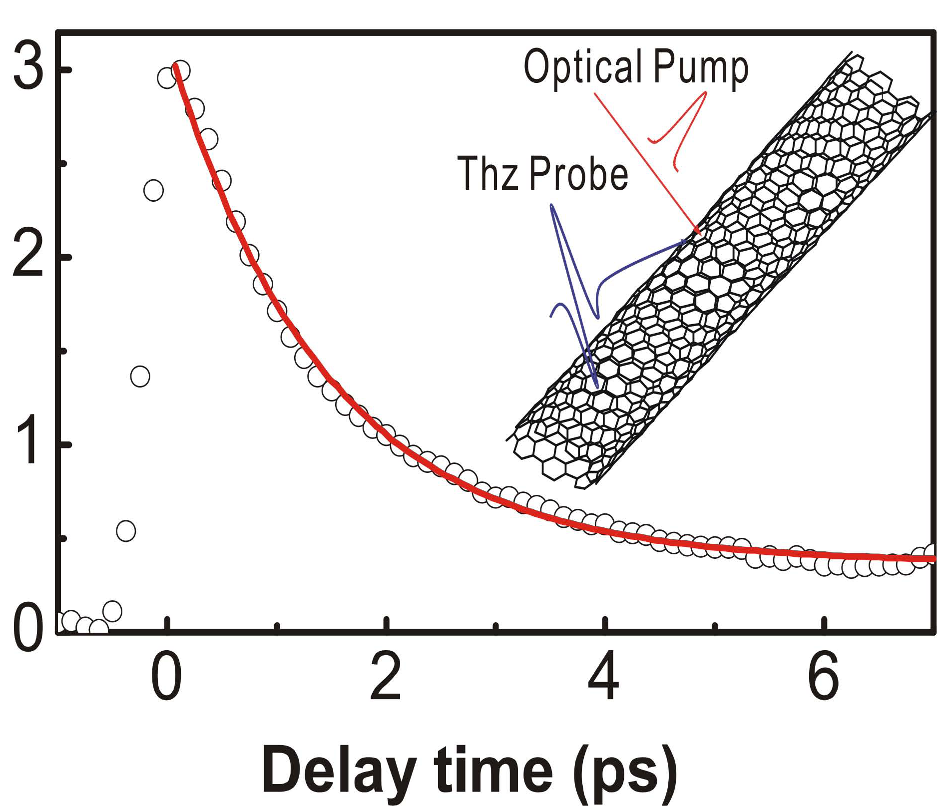 | X Xu, K Chuang, RJ Nicholas, MB Johnston, LM Herz
J. Phys. Chem. C, 113:18106--18109 (Sep 2009)
[
pdf ][ SI ][ ref ]
We have investigated the ultrafast far-infrared transmission of isolated single-walled carbon nanotubes using optical-pump THz-probe spectroscopy. The THz dielectric response is dominated by excitons with an initial, rapid decay due to Auger recombination followed by a slow decay of isolated single excitons. Frequency-dependent analysis of the photoinduced dielectric function suggest an internal excitonic excitation at 11 meV with further low-frequency (0.6 and 1.4 THz) absorption features at high densities ascribed to exciton complexes. A featureless conductivity bleaching is attributed to an exciton-induced reduction in the mobility of free carriers caused by phase-space filling.
Citations: 37 (Scopus) 35 (Web of Science) |
- Photoconductive response correction for detectors of terahertz radiation
-
 | E Castro-Camus, L Fu, J Lloyd-Hughes, HH Tan, C Jagadish, MB Johnston
J. Appl. Phys., 104:053113 (Sep 2008)
[
pdf ][ SI ][ ref ]
Photoconductive detectors are convenient devices for detecting pulsed terahertz radiation. We have optimized Fe+ ion-damaged InP materials for photoconductive detector signal to noise performance using dual-energy doses in the range from 2.5×10¹² to 1.0×1016 cm−2. Ion implantation allowed the production of semiconducting materials with free-carrier lifetimes between 0.5 and 2.1 ps, which were measured by optical pump terahertz probe spectroscopy. The time resolved photoconductivity of the detector substrates was acquired as a function of time after excitation by 2 nJ pulses from a laser oscillator. These data, when combined with a deconvolution algorithm, provide an excellent spectral response correction to the raw photocurrent signal recorded by the photoconductive detectors.
Citations: 58 (Scopus) 59 (Web of Science) |
- Efficient generation of charges via below-gap photoexcitation of polymer-fullerene blend films investigated by terahertz spectroscopy
-
 | P Parkinson, J Lloyd-Hughes, MB Johnston, LM Herz
Phys. Rev. B, 78:115321 (Sep 2008)
[
pdf ][ SI ][ ref ]
Using optical-pump terahertz-probe spectroscopy, we have investigated the time-resolved conductivity dynamics of photoexcited polymer-fullerene bulk heterojunction blends for two model polymers: poly[3-hexylthiophene] (P3HT) and poly[2-methoxy-5-(-dimethyloctyloxy)-1,4-phenylenevinylene] (MDMO-PPV) blended with [6,6]-phenyl-C61 butyric acid methyl ester (PCBM). The observed terahertz-frequency conductivity is characteristic of dispersive charge transport for photoexcitation both at the −* absorption peak (560 nm for P3HT) and significantly below it (800 nm). The photoconductivity at 800 nm is unexpectedly high, which we attribute to the presence of a charge-transfer complex. We report the excitation-fluence dependence of the photoconductivity over more than four orders of magnitude, obtained by utilizing a terahertz spectrometer based upon on either a laser oscillator or an amplifier source. The time-averaged photoconductivity of the P3HT:PCBM blend is over 20 times larger than that of P3HT, indicating that long-lived hole polarons are responsible for the high photovoltaic efficiency of polymer:fullerene blends. At early times (~ps) the linear dependence of photoconductivity upon fluence indicates that interfacial charge transfer dominates as an exciton decay pathway, generating charges with mobility of at least ~0.1 cm2 V−1 s−1. At later times, a sublinear relationship shows that carrier-carrier recombination effects influence the conductivity on a longer time scale (>1 µs) with a bimolecular charge annihilation constant for the blends that is approximately two to three orders of magnitude smaller than that typical for neat polymer films.
Citations: 98 (Scopus) 100 (Web of Science) |
- Conductivity of nanoporous {InP} membranes investigated using terahertz spectroscopy
-
 | SKE Merchant, J Lloyd-Hughes, L Sirbu, IM Tiginyanu, P Parkinson, LM Herz, MB Johnston
Nanotechnology, 19:395704 (Aug 2008)
[
pdf ][ SI ][ ref ]
We have investigated the terahertz conductivity of extrinsic and photoexcited electrons in nanoporous indium phosphide (InP) at different pore densities and orientations. The form of electronic transport in the film was found to differ significantly from that for bulk InP. While photo-generated electrons showed Drude-like transport, the behaviour for extrinsic electrons deviated significantly from the Drude model. Time-resolved photoconductivity measurements found that carrier recombination was slow, with lifetimes exceeding 1~ns for all porosities and orientations. When considered together, these findings suggest that the surfaces created by the nanopores strongly alter the dynamics of both extrinsic and photoexcited electrons.
Citations: 17 (Scopus) 18 (Web of Science) |
- Terahertz photoconductivity of mobile electrons in nanoporous {InP} honeycombs
-
 | J Lloyd-Hughes, SKE Merchant, L Sirbu, IM Tiginyanu, MB Johnston
Phys. Rev. B, 78:085320 (Aug 2008)
[
pdf ][ SI ][ ref ]
Nanostructured semiconductors with favorable optoelectronic properties can be created by electrochemical etching, a fabrication process that is scalable for mass market applications. Using terahertz photoconductivity measurements, we demonstrate that nanoporous InP has an unusually long carrier recombination lifetime that exceeds 100 ns at low temperatures and low carrier density, and an electron mobility half that of bulk InP. Modeling confirms that these observations result from band bending with holes confined to the surface and electrons away from the pores.
Citations: 19 (Scopus) 16 (Web of Science) |
- Low-energy collective dynamics of charge stripes in the doped nickelate {La}$_{2-x}${Sr}$_{x}${NiO}$_{4+\delta}$ observed with optical conductivity measurements
-
 | J Lloyd-Hughes, D Prabhakaran, AT Boothroyd, MB Johnston
Phys. Rev. B, 77:195114 (May 2008)
[
pdf ][ SI ][ ref ]
We have investigated charge dynamics in the static stripe ordered phase of La_{2-x}Sr_{x}NiO_{4+\\delta} at lattice temperatures below the charge ordering transition, via optical conductivity measurements at low energies (1 – 10 meV). The thermally activated dynamic response of the charge stripes is found to be characteristic of a collective mode such as a pinned charge density wave. At incommensurate doping levels, the pinning energy is reduced, owing to the presence of real-space defects in the stripe order, and a pronounced increase in the oscillator strength is seen. The results provide compelling evidence for the existence of low-energy collective modes of the charge stripes.
Citations: 10 (Scopus) 11 (Web of Science) |
- Conformational changes of photoactive yellow protein monitored by terahertz spectroscopy
-
 | E Castro-Camus, MB Johnston
Chem. Phys. Lett., 455:289-292 (Apr 2008)
[
pdf ][ SI ][ ref ]
Observing the structural dynamics of proteins under conditions as close as possible to those in a living organism is essential for understanding the biological functions of proteins accurately. Here we demonstrate that terahertz spectroscopy is a convenient probe of conformational changes in proteins suspended in physiological buffer solution. We have observed that the partial unfolding of photoactive yellow protein leads to a clear increase in absorption at terahertz frequencies. Using normal mode and molecular dynamics simulations we show that this increase in absorption is related to an increase in the density of delocalised vibrational modes in the more flexible partially unfolded state.
Citations: 70 (Scopus) 61 (Web of Science) |
- Exciton dissociation in polymer field-effect transistors studied using terahertz spectroscopy
-
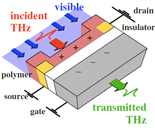 | J Lloyd-Hughes, T Richards, H Sirringhaus, MB Johnston, LM Herz
Phys. Rev. B, 77:125203 (Mar 2008)
[
pdf ][ SI ][ ref ]
We have used terahertz time-domain spectroscopy to investigate photoinduced charge generation in conjugated polymer field-effect transistors. Our measurements show that excitons dissociate in the accumulation layer under the application of a gate voltage, with a quantum efficiency of ~0.1 for an average gate field of ~1×10^8 Vm-1. The transistor history is found to affect the exciton dissociation efficiency, which decreases as holes are increasingly trapped in the accumulation layer. The quantum efficiency of charge formation from excitons is compared with the two contrasting models proposed by Onsager and Arkhipov based on the assumption that field-induced exciton dissociation is assisted by the Brownian diffusive motion or an initial excess energy supplied by excited vibrational modes, respectively.
|
- Terahertz magnetoconductivity of excitons and electrons in quantum cascade structures
-
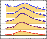 | J Lloyd-Hughes, HE Beere, DA Ritchie, MB Johnston
Phys. Rev. B, 77:125322 (Mar 2008)
[
pdf ][ SI ][ ref ]
We examined the quasiparticles formed by the photoexcitation of GaAs/AlGaAs terahertz quantum cascade structures using terahertz time-domain spectroscopy. At low temperature and excitation density the measured conductivity was excitonic, with a 1s-2p transition energy indicative of three-dimensional excitons correlated across the quantum well barriers. Free electrons increasingly dominated the conductive response at higher lattice temperatures and excitation densities. Under an external magnetic field transitions from the 1s level into 2p states with different magnetic quantum number were observed, while at high excitation densities the electron cyclotron resonance became more prominent.
Citations: 21 (Scopus) 20 (Web of Science) |
- Excitation-density-dependent generation of broadband terahertz radiation in an asymmetrically excited photoconductive antenna
-
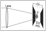 | PC Upadhya, W Fan, A Burnett, J Cunningham, AG Davies, EH Linfield, J Lloyd-Hughes, E Castro-Camus, MB Johnston, H Beere
Opt. Lett., 32:2297 (Aug 2007)
[
pdf ][ SI ][ ref ]
The generation of terahertz (THz) transients in photoconductive emitters has been studied by varying the spatial extent and density of the optically excited photocarriers in asymmetrically excited, biased low-temperature-grown GaAs antenna structures. We find a pronounced dependence of the THz pulse intensity and broadband (>6.0 THz) spectral distribution on the pump excitation density and simulate this with a three-dimensional carrier dynamics model. We attribute the observed variation in THz emission to changes in the strength of the screening field.
Citations: 59 (Scopus) 52 (Web of Science) |
- Transient terahertz conductivity of {GaAs} nanowires
-
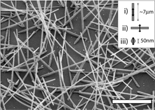 | P Parkinson, J Lloyd-Hughes, Q Gao, HH Tan, C Jagadish, MB Johnston, LM Herz
Nano Lett., 7:2162-2165 (Jul 2007)
[
pdf ][ SI ][ ref ]
The time-resolved conductivity of isolated GaAs nanowires is investigated by optical-pump terahertz-probe time-domain spectroscopy. The electronic response exhibits a pronounced surface plasmon mode that forms within 300 fs before decaying within 10 ps as a result of charge trapping at the nanowire surface. The mobility is extracted using the Drude model for a plasmon and found to be remarkably high, being roughly one-third of that typical for bulk GaAs at room temperature.
Citations: 210 (Scopus) 190 (Web of Science) |
- An ion-implanted InP receiver for polarization resolved terahertz spectroscopy
-
 | E Castro-Camus, J Lloyd-Hughes, L Fu, HH Tan, C Jagadish, MB Johnston
Opt. Express, 15:7047-7057 (May 2007)
[
pdf ][ SI ][ ref ]
We report on the construction, optical alignment and performance of a receiver which is capable of recording the full polarization state of coherent terahertz radiation. The photoconductive detector was fabricated on InP which had been implanted with Fe+ ions. The device operated successfully when it was gated with near infrared femtosecond pulses from either a Ti:sapphire laser oscillator or a 1 kHz regenerative laser amplifier. When illuminated with terahertz radiation from a typical photoconductive source, the optimized device had a signal to noise figure of 100:1 with a usable spectral bandwidth of up to 4 THz. The device was shown to be very sensitive to terahertz polarization, being able to resolve changes in polarization of 0.34 degrees. Additionally, we have demonstrated the usefulness of this device for (i) polarization sensitive terahertz spectroscopy, by measuring the birefringence of quartz and (ii) terahertz emission experiments, by measuring the polarization dependence of radiation generated by optical rectification in (110)-ZnTe.
Citations: 51 (Scopus) 48 (Web of Science) |
- Plasmonics: Superfocusing of terahertz waves
-
 | MB Johnston
Nat. Photon., 1:14-15 (Jan 2007)
[
pdf ][ SI ][ ref ]
The promising field of terahertz imaging has long been limited by poor resolution. Researchers now believe that the intriguing properties of surface-plasmon polaritons on corrugated wires could help beat the diffraction limit and inspire a new generation of terahertz photonic devices.
Citations: 49 (Scopus) 46 (Web of Science) |
- Influence of surface passivation on ultrafast carrier dynamics and terahertz radiation generation in GaAs
-
 | J Lloyd-Hughes, SKE Merchant, L Fu, HH Tan, C Jagadish, E Castro-Camus, MB Johnston
Appl. Phys. Lett., 89:232102 (Dec 2006)
[
pdf ][ SI ][ ref ]
The carrier dynamics of photoexcited electrons in the vicinity of the surface of (NH4)(2)S-passivated GaAs were studied via terahertz emission spectroscopy and optical-pump terahertz-probe spectroscopy. Terahertz emission spectroscopy measurements, coupled with Monte Carlo simulations of terahertz emission, revealed that the surface electric field of GaAs reverses after passivation. The conductivity of photoexcited electrons was determined via optical-pump terahertz-probe spectroscopy and was found to double after passivation. These experiments demonstrate that passivation significantly reduces the surface state density and surface recombination velocity of GaAs. Finally, it was demonstrated that passivation leads to an enhancement in the power radiated by photoconductive switch terahertz emitters, thereby showing the important influence of surface chemistry on the performance of ultrafast terahertz photonic devices. (c) 2006 American Institute of Physics.
Citations: 109 (Scopus) 94 (Web of Science) |
- Charge trapping in polymer transistors probed by terahertz spectroscopy and scanning probe potentiometry
-
 | J Lloyd-Hughes, T Richards, H Sirringhaus, E Castro-Camus, LM Herz, MB Johnston
Appl. Phys. Lett., 89:112101 (Sep 2006)
[
pdf ][ SI ][ ref ]
Terahertz time-domain spectroscopy and scanning probe potentiometry were used to investigate charge trapping in polymer field-effect transistors fabricated on a silicon gate. The hole density in the transistor channel was determined from the reduction in the transmitted terahertz radiation under an applied gate voltage. Prolonged device operation creates an exponential decay in the differential terahertz transmission, compatible with an increase in the density of trapped holes in the polymer channel. Taken in combination with scanning probe potentiometry measurements, these results indicate that device degradation is largely a consequence of hole trapping, rather than of changes to the mobility of free holes in the polymer.
Citations: 16 (Scopus) 12 (Web of Science) |
- Longitudinal electron bunch profile diagnostics at 45MeV using coherent Smith-Purcell radiation
-
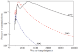 | G Doucas, V Blackmore, B Ottewell, C Perry, PG Huggard, E Castro-Camus, MB Johnston, J Lloyd-Hughes, MF Kimmitt, B Redlich, A van der Meer
Phys. Rev. Spec. Top.-Accel. Beams, 9:092801 (Sep 2006)
[
pdf ][ SI ][ ref ]
We have used coherent Smith-Purcell radiation in order to investigate the longitudinal ( temporal) profile of the electron bunch at the FELIX facility. Detection of the far-infrared radiation was achieved by a simple and compact experimental arrangement, consisting of an array of 11 room-temperature pyroelectric detectors. Accurate determination of the background radiation, use of high quality optical filters, and an efficient light collection system are essential for this type of experiment. The radiated power is in good agreement with the predictions of the surface current description of this process. It is concluded that 90% of the bunch particles are contained within 5.5 ps, with a temporal profile that could be approximately triangular in shape.
Citations: 57 (Scopus) 44 (Web of Science) |
- Simulation and optimisation of terahertz emission from InGaAs and InP
photoconductive switches
-
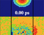 | J Lloyd-Hughes, E Castro-Camus, MB Johnston
Solid State Commun., 136:595-600 (Dec 2005)
[
pdf ][ SI ][ ref ]
We simulate the terahertz emission from laterally biased InGaAs and InP using a three-dimensional carrier dynamics model in order to optimise the semiconductor material. Incident pump-pulse parameters of current Ti:Sapphire and Er:fibre lasers are chosen, and the simulation models the semiconductor\'s bandstructure using parabolic T, L and X valleys, and heavy holes. The emitted terahertz radiation is propagated within the semiconductor and into free space using a model based on the Drude-Lorentz dielectric function. As the InGaAs alloy approaches InAs an increase in the emitted power is observed, and this is attributed to a greater electron mobility. Additionally, low-temperature grown and ion-implanted InGaAs are modelled using a finite carrier trapping time. At sub-picosecond trapping times the terahertz bandwidth is found to increase significantly at the cost of a reduced emission power.
Citations: 46 (Scopus) 40 (Web of Science) |
- Polarization-sensitive terahertz detection by multicontact
photoconductive receivers
-
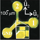 | E Castro-Camus, J Lloyd-Hughes, MB Johnston, MD Fraser, HH Tan, C Jagadish
Appl. Phys. Lett., 86:254102 (Jun 2005)
[
pdf ][ SI ][ ref ]
We have developed a terahertz radiation detector that measures both the amplitude and polarization of the electric field as a function of time. The device is a three-contact photoconductive receiver designed so that two orthogonal electric-field components of an arbitrary polarized electromagnetic wave may be detected simultaneously. The detector was fabricated on Fe+ ion-implanted InP. Polarization-sensitive detection is demonstrated with an extinction ratio better than 100:1. This type of device will have immediate application in studies of birefringent and optically active materials in the far-infrared region of the spectrum. (c) 2005 American Institute of Physics.
Citations: 146 (Scopus) 128 (Web of Science) |
- Three-dimensional carrier-dynamics simulation of terahertz emission
from photoconductive switches
-
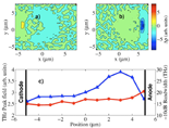 | E Castro-Camus, J Lloyd-Hughes, MB Johnston
Phys. Rev. B, 71:195301 (May 2005)
[
pdf ][ SI ][ ref ]
A semi-classical Monte Carlo model for studying three-dimensional carrier dynamics in photoconductive switches is presented. The model was used to simulate the process of photoexcitation in GaAs-based photoconductive antennas illuminated with pulses typical of mode-locked Ti:Sapphire lasers, We analyzed the power and frequency bandwidth of THz radiation emitted from these devices as a function of bias voltage. pump pulse duration and pump pulse location. We show that the mechanisms limiting the THz power emitted from photoconductive switches fall into two regimes: when illuminated with short duration (< 40 fs) laser pulses the energy distribution of the Gaussian pulses constrains the emitted power. while for long (> 40 fs) pulses, screening is the primary power-limiting mechanism. A discussion of the dynamics of bias field screening in the gap region is presented, The emitted terahertz power was found to be enhanced when the exciting laser pulse was in close proximity to the anode of the photoconductive emitter, in agreement with experimental results, We show that this enhancement arises from the electric field distribution within the emitter combined with a difference in the mobilities of electrons and holes.
Citations: 95 (Scopus) 80 (Web of Science) |
- Carrier dynamics in ion-implanted GaAs studied by simulation and
observation of terahertz emission
-
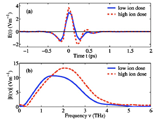 | J Lloyd-Hughes, E Castro-Camus, MD Fraser, C Jagadish, MB Johnston
Phys. Rev. B, 70:235330 (Dec 2004)
[
pdf ][ SI ][ ref ]
We have studied terahertz (THz) emission from arsenic-ion implanted GaAs both experimentally and using a three-dimensional carrier dynamics simulation. A uniform density of vacancies was formed over the optical absorption depth of bulk GaAs samples by performing multienergy implantations of arsenic ions (1 and 2.4 MeV) and subsequent thermal annealing. In a series of THz emission experiments the frequency of peak THz power was found to increase significantly from 1.4 to 2.2 THz when the ion implantation dose was increased from 10(13) to 10(16) cm(-3). We used a semiclassical Monte Carlo simulation of ultrafast carrier dynamics to reproduce and explain these results. The effect of the ion-induced damage was included in the simulation by considering carrier scattering at neutral and charged impurities, as well as carrier trapping at defect sites. Higher vacancy concentrations and shorter carrier trapping times both contributed to shorter simulated THz pulses, the latter being more important over experimentally realistic parameter ranges.
Citations: 60 (Scopus) 51 (Web of Science) |
- Emission of collimated THz pulses from photo-excited semiconductors
-
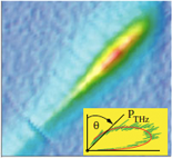 | MB Johnston, A Dowd, R Driver, EH Linfield, AG Davies, DM Whittaker
Semicond. Sci. Technol., 19:S449-S451 (Apr 2004)
[
pdf ][ SI ][ ref ]
It is shown experimentally that surface-field terahertz (THz) emitters can produce well-collimated beams of THz radiation, making them useful devices for time-domain spectroscopy applications. Simulations of the carrier-dynamics are used to explain the mechanism of THz generation in InAs and GaAs, and it is shown that inter-valley scattering of electrons must be considered in order to fully describe THz emission from InAs.
Citations: 20 (Scopus) 19 (Web of Science) |
- Selective dielectrophoretic manipulation of surface-immobilized DNA
molecules
-
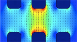 | WA Germishuizen, C Walti, R Wirtz, MB Johnston, M Pepper, AG Davies, APJ Middelberg
Nanotechnology, 14:896-902 (Aug 2003)
[
pdf ][ SI ][ ref ]
The fabrication of nanoscale molecular devices is becoming increasingly important and research into their fabrication has intensified over the last few years. In particular, the attachment of molecular objects onto various surfaces has attracted considerable attention. Here, we report a multistep surface immobilization procedure, which allows the specific and controlled attachment of very long DNA molecules onto gold electrodes. Further, we report the effect of dielectrophoresis on these surface-bound DNA molecules with respect to amplitude and frequency, and we show that selected surface-immobilized DNA molecules can be manipulated by dielectrophoresis. Finally, we investigated the use of dielectrophoresis in conjunction with the multistep surface immobilization of fluorescently labelled, surface-bound lambda-DNA in a basic data-storage device.
Citations: 56 (Scopus) 50 (Web of Science) |
- Low-energy vibrational modes in phenylene oligomers studied by THz
time-domain spectroscopy
-
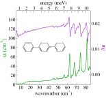 | MB Johnston, LM Herz, ALT Khan, A Kohler, AG Davies, EH Linfield
Chem. Phys. Lett., 377:256-262 (Aug 2003)
[
pdf ][ SI ][ ref ]
Low-energy vibrational modes have been investigated in polycrystalline biphenyl, para-terphenyl, para-quaterphenyl and para-sexiphenyl using THz time-domain spectroscopy (THz-TDS). A number of both internal and external infrared-active modes were observed for wavenumbers ranging between 20 and 80 cm(-1). The temperature dependence of these modes is consistent with structural phase transitions occurring in the molecular crystal, indicating that THz-TDS is a sensitive probe of the conformation of conjugated molecular systems. (C) 2003 Elsevier B.V. All rights reserved.
Citations: 99 (Scopus) 90 (Web of Science) |
- The development of terahertz sources and their applications
-
 | AG Davies, EH Linfield, MB Johnston
Phys. Med. Biol., 47:3679-3689 (Nov 2002)
[
pdf ][ SI ][ ref ]
The terahertz region of the electromagnetic spectrum spans the frequency range between the mid-infrared and the millimetre/microwave. This region has not been exploited fully to date owing to the limited number of suitable (in particular. coherent) radiation sources and detectors. Recent demonstrations,, using pulsed near-infrared femtosecond laser systems, of the viability of THz medical imaging and spectroscopy have sparked international interests yet much research still needs to be undertaken to optimize both the power and bandwidth in such THz systems. In this paper, we review how femtosecond near-infrared laser pulses can be converted into broad band THz radiation using semiconductor crystals. and discuss in depth the optimization of one specific generation mechanism based on ultra-fast transport of electrons and holes at a semiconductor surface. We also outline a few of the opportunities for a technology that can address a diverse range of challenges spanning the physical and biological sciences, and note the continuing need for the development of solid state, continuous wave. THz sources which operate at room temperature.
Citations: 158 (Scopus) 139 (Web of Science) |
- Generation of high-power terahertz pulses in a prism
-
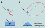 | MB Johnston, DM Whittaker, A Dowd, AG Davies, EH Linfield, X Li, DA Ritchie
Opt. Lett., 27:1935-1937 (Nov 2002)
[
pdf ][ SI ][ ref ]
A compact, high-power emitter of half-cycle terahertz (THz) radiation is demonstrated. The device consists of an epitaxial InAs emitter upon a GaAs prism and produces THz pulses that are 20 times more powerful than those from conventional planar InAs emitters. This improvement is a direct result of reorienting the transient THz dipole such that its axis is not perpendicular to the emitting surface. (C) 2002 Optical Society of America.
Citations: 52 (Scopus) 46 (Web of Science) |
- Simulation of terahertz generation at semiconductor surfaces
-
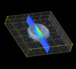 | MB Johnston, DM Whittaker, A Corchia, AG Davies, EH Linfield
Phys. Rev. B, 65:165301 (Apr 2002)
[
pdf ][ SI ][ ref ]
A three-dimensional semiclassical Monte Carlo model is presented to describe fast carrier dynamics in semiconductors after photoexcitation. Far-field terahertz (THz) radiation patterns are calculated for both InAs and GaAs with, and without, application of external magnetic fields. This analysis distinguishes between surface depletion field and photo-Dember mechanisms for generating THz radiation. The theoretical model reproduces experimental data from GaAs and InAs, and demonstrates that a magnetic field enhances THz emission by rotating the emitting dipole with respect to the sample surface, leading to an increased coupling of radiation through the surface.
Citations: 307 (Scopus) 311 (Web of Science) |
- Magnetic-field-induced enhancement of terahertz emission from III-V
semiconductor surfaces
-
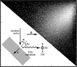 | MB Johnston, A Corchia, A Dowd, EH Linfield, AG Davies, R McLaughlin, DD Arnone, M Pepper
Physica E, 13:896-899 (Mar 2002)
[
pdf ][ SI ][ ref ]
We discuss the origins of the magnetic - field-induced enhancement of terahertz (THz) emission from bulk semiconductor surfaces. The principal effect of the magnetic field is to rotate the THz dipole and hence dramatically increase the THz power radiated through the semiconductor surface. It also significantly affects the ability of the photo-created carriers to screen surface electric fields. The sensitivity of THz emission to the motion of photo-created carriers makes this an ideal probe of hot carrier dynamics both in bulk semiconductors and sophisticated heterostructures. (C) 2002 Elsevier Science B.V. All rights reserved.
Citations: 16 (Scopus) 14 (Web of Science) |
- Thermally stimulated luminescence in ion-implanted GaAs
-
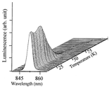 | M Gal, LV Dao, E Kraft, MB Johnston, C Carmody, HH Tan, C Jagadish
J. Lumines., 96:287-293 (Mar 2002)
[
pdf ][ SI ][ ref ]
We have studied the temperature dependence of the luminescence of ion implanted GaAs between 10 and 300 K. We found that at certain temperatures the luminescence increases with increasing temperature. We attribute these localised increases in the luminescence intensity to the thermal excitation of carriers out of traps, or in other words, to thermally stimulated luminescence or thermoluminescence. Model calculations which include thermoluminescence produce excellent agreement with the experimental data and allow us to determine the trap parameters. (C) 2002 Elsevier Science B.V. All rights reserved.
|
- Theory of magnetic-field enhancement of surface-field terahertz emission
-
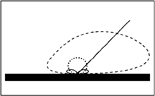 | MB Johnston, DM Whittaker, A Corchia, AG Davies, EH Linfield
J. Appl. Phys., 91:2104-2106 (Feb 2002)
[
pdf ][ SI ][ ref ]
We present a theoretical treatment of surface-field THz generation in semiconductors, which explains the power enhancement observed when a magnetic field is applied. Our model consists of two parts: a Monte Carlo simulation of the dynamics of carriers generated by a subpicosecond optical pulse, and a calculation of the resulting THz radiation emitted through the semiconductor surface. The magnetic field deflects the motion of the carriers, producing a component of the THz dipole parallel to the surface. This causes the power transmitted through the surface to be increased by more than one order of magnitude. (C) 2002 American Institute of Physics.
Citations: 66 (Scopus) 63 (Web of Science) |
- Effects of magnetic field and optical fluence on terahertz emission in
gallium arsenide
-
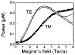 | A Corchia, R McLaughlin, MB Johnston, DM Whittaker, DD Arnone, EH Linfield, AG Davies, M Pepper
Phys. Rev. B, 6420:205204 (Nov 2001)
[
pdf ][ SI ][ ref ]
The excitation density dependence of magnetic-field-enhanced terahertz (THz=10(12) Hz) emission from (100) GaAs is studied. It is found that THz power saturates at a higher optical-excitation density, when a magnetic field is applied. This observation explains the different magnetic field enhancements that have been reported recently. At low excitation densities the results are shown to be consistent with a simple model of carrier-carrier scattering, whilst at higher densities surface field screening becomes important.
Citations: 0 (Scopus) 24 (Web of Science) |
- Carrier capture and relaxation in Stranski-Krastanow
InxGa1-xAs/GaAs(311)B quantum dots
-
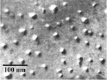 | C Lobo, N Perret, D Morris, J Zou, DJH Cockayne, MB Johnston, M Gal, R Leon
Phys. Rev. B, 62:2737-2742 (Jul 2000)
[
pdf ][ SI ][ ref ]
We have investigated the structure and optical properties of In0.6Ga0.4As/GaAs(311)B quantum dots (QD'''s) formed by the Stranski-Krastanow growth mode during metal-organic chemical-vapor deposition. We find that (311)B QD structures display a higher energy QD luminescence emission and a stronger wetting-layer emission than (100) QD'''s of similar diameter and density. Temperature-dependent photoluminescence (PL) measurements reveal shallow QD confinement energies and strong interaction between neighboring quantum dots. Longer PL rise times of the ground-state emission of (311)B QD'''s compared to (100) QD'''s are ascribed to the effect of differing numbers, energies, and level spacings of QD confined states on intersublevel relaxation mechanisms at low-carrier excitation densities.
Citations: 23 (Scopus) 20 (Web of Science) |
- Enhanced coherent terahertz emission from indium arsenide in the
presence of a magnetic field
-
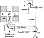 | R McLaughlin, A Corchia, MB Johnston, Q Chen, CM Ciesla, DD Arnone, GAC Jones, EH Linfield, AG Davies, M Pepper
Appl. Phys. Lett., 76:2038-2040 (Apr 2000)
[
pdf ][ SI ][ ref ]
We demonstrate enhancement of terahertz (THz) emission from indium arsenide at 170 K in magnetic fields (B) up to 8 T. An order of magnitude increase in visible to terahertz conversion efficiency was observed, with no suggestion of saturation of the TE polarization at higher magnetic fields. Free-space electro-optic sampling measurements confirmed the coherent nature of this radiation over the field range investigated, and gave an insight into the carrier motion subsequent to photoexcitation, which may be responsible for the observed THz power enhancement. (C) 2000 American Institute of Physics. [S0003-6951(00)03115-6].
Citations: 102 (Scopus) 90 (Web of Science) |
- Wavelength shifting of adjacent quantum wells in V-groove quantum wire
structure by selective implantation and annealing
-
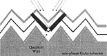 | XQ Liu, W Lu, XS Chen, SC Shen, HH Tan, S Yuan, C Jagadish, MB Johnston, LV Dao, M Gal, J Zou, DJH Cockayne
J. Appl. Phys., 87:1566-1568 (Feb 2000)
[
pdf ][ SI ][ ref ]
Intermixing induced by selective implantation was used to modify the two-dimensional (2D) quantum wells in the V-grooved quantum wire structure. Photoluminescence measurement of the implanted samples shows the obvious blueshift of the interband transition energy while quantum wire is not influenced by implantation. So the selective implantation method has been demonstrated in this article as a useful technique to isolate the energy levels of quantum wire structure from its neighbor 2D structures, which is preferred for the optoelectronic device application of quantum wire. (C) 2000 American Institute of Physics. [S0021-8979(00)02703-1].
|
- Proton implantation and rapid thermal annealing effects on GaAs/AlGaAs
quantum well infrared photodetectors
-
 | N Li, N Li, W Lu, XQ Liu, XZ Yuan, ZF Li, HF Dou, SC Shen, Y Fu, M Willander, L Fu, HH Tan, C Jagadish, MB Johnston, M Gal
Superlattices Microstruct., 26:317-324 (Nov 1999)
[
pdf ][ SI ][ ref ]
We report the use of intermixing techniques to modify GaAs/AlGaAs multiple quantum wells (MQWs). A large shift in the response wavelength of the GaAs/AlGaAs MQW-based infrared photodetector is obtained by proton implantation and then a standard annealing procedure (950 degrees C for 30 s). The photoluminescence (PL) and photoresponse spectra were measured as functions of ion dose in the range from 5 x 10(14) to 2.5 x 10(15) cm(-3). The peak photoresponse wavelength was tunable between 8.2 and 9.8 mu m for the infrared radiation and the energy position of the PL peak from the MQW material changed from 1.62 to 1.645 eV. The effects of the ion implantation and thermal annealing on the device performance have been well characterized theoretically by the inter-diffusion of Al atoms across the GaAs/AlGaAs heterointerfaces and the relaxation energy of free carriers. (C) 1999 Academic Press.
Citations: 15 (Scopus) 13 (Web of Science) |
- Interdiffused quantum-well infrared photodetectors for color sensitive
arrays
-
 | MB Johnston, M Gal, N Li, ZH Chen, XQ Liu, N Li, W Lu, SC Shen, L Fu, HH Tan, C Jagadish
Appl. Phys. Lett., 75:923-925 (Aug 1999)
[
pdf ][ SI ][ ref ]
Proton implantation and rapid thermal annealing were used to tune the infrared spectral response of quantum-well infrared photodetectors (QWIP) by up to 1.4 mu m. Multiple proton implants at energies between 200 and 420 keV were used to create homogeneous quantum-well intermixing throughout the device'''s multiple-quantum-well structure. Photoluminescence and spectral response measurements were used to study the effect of proton implantation on QWIPs for a series of doses up to 3.5x10(15) protons cm(-2). By using a mask during implantation, a method of constructing a color sensitive array is proposed. (C) 1999 American Institute of Physics. [S0003-6951(99)02333-5].
Citations: 23 (Scopus) 22 (Web of Science) |
- Proton irradiation-induced intermixing in InGaAs/(Al)GaAs quantum wells
and quantum-well lasers
-
 | L Fu, HH Tan, MB Johnston, M Gal, C Jagadish
J. Appl. Phys., 85:6786-6789 (May 1999)
[
pdf ][ SI ][ ref ]
Proton irradiation with subsequent rapid thermal annealing was used to investigate intermixing of InGaAs/GaAs and InGaAs/AlGaAs quantum wells. Large photoluminescence (PL) energy shifts were observed in both materials. Comparatively, InGaAs/AlGaAs samples showed larger PL energy shifts than InGaAs/GaAs samples because of the presence of Al in the barriers and also better recovery of PL intensities, which is mainly due to dynamic annealing effects in AlGaAs during irradiation. Based on this, InGaAs/AlGaAs quantum-well lasers were fabricated and up to 49.3-nm-emission wavelength shift was observed in the proton-irradiated laser with no significant degradation in device characteristics. (C) 1999 American Institute of Physics. [S0021-8979(99)09609-7].
Citations: 37 (Scopus) 38 (Web of Science) |
- Si and C delta-doping for device applications
-
 | G Li, MB Johnston, A Babinski, S Yuan, M Gal, SJ Chua, C Jagadish
J. Cryst. Growth, 195:54-57 (Dec 1998)
[
pdf ][ SI ][ ref ]
Growth conditions have been optimised for Si and C delta-doped AlGaAs at 630 degrees C. Very high free carrier densities up to 6 x 10(18) and 3 x 10(19) cm(-3), respectively, for Si and C delta-doped AlGaAs, were obtained. The key parameters to precisely control delta-doping concentrations were discussed. Growth of high quality Si and C delta-doped nipi structures, Si delta-modulation doped In0.2Ca0.8As/GaAs quantum wells, and high performance Zn-free C delta-doped In0.2Ga0.8As/GaAs GRINSCH lasers were also reported. (C) 1998 Elsevier Science B.V. All rights reserved.
|
- Improved carrier collection in intermixed InGaAs/GaAs quantum wells
-
 | LV Dao, MB Johnston, M Gal, L Fu, HH Tan, C Jagadish
Appl. Phys. Lett., 73:3408-3410 (Dec 1998)
[
pdf ][ SI ][ ref ]
We have used photoluminescence up conversion to study the carrier capture times into intermixed InGaAs/GaAs quantum wells. We have found that the capture into the intermixed wells is markedly faster than capture into the reference (unintermixed) quantum wells. The reasons for the significant reduction in the capture time is related to the shape of the intermixed quantum well. Such a reduction in the capture time is beneficial both in terms of the quantum efficiency and the frequency response of intermixed optoelectronic devices. (C) 1998 American Institute of Physics. [S0003-6951(98)01849-X].
Citations: 27 (Scopus) 27 (Web of Science) |
- Si and C delta-doping of GaAs grown by metal organic vapour phase
epitaxy for fabrication of nipi doping superlattices
-
 | C Jagadish, G Li, MB Johnston, M Gal
Mater. Sci. Eng. B-Solid State Mater. Adv. Technol., 51:103-105 (Feb 1998)
[
pdf ][ SI ][ ref ]
The growth conditions for Si and C delta-doped nipi doping superlattices in GaAs have been optimised at the growth temperature of 630 degrees C. We found that the Si delta-doping concentration can be significantly changed by delta-doping time over the range of 10(12)-10(13) cm(-2) at the optimised gas flow velocity. The similar range of the free hole density in C delta-doped GaAs has also been obtained simply by varying the TMAl flow rate during the delta-doping step. The full compensation of free electron and hole density in the Si and C delta-doped nipis can be achieved by choosing proper Si delta-doping time and TMAl flow rate. Growth of one Si and C delta-doped nipi in GaAs was demonstrated. Apart from the well-known effect of photo-excitation intensity on the effective band gap energy, the time-resolved photoluminescence reveals that the photoluminescence peak wavelength significantly increases in the relaxation process of the photo-excited nipi doping superlattice. (C) 1998 Elsevier Science S.A. All rights reserved.
|
- Photoluminescence study of the dynamical properties of GaAs sawtooth
superlattices
-
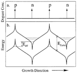 | MB Johnston, M Gal, G Li, C Jagadish
J. Appl. Phys., 82:5748-5752 (Dec 1997)
[
pdf ][ SI ][ ref ]
The dynamic properties of a sawtooth superlattice (delta-doped nipi) were examined by photoluminescence (PL) spectroscopic techniques, The structure was grown on a semi-insulating GaAs substrate by metalorganic vapor phase epitaxy, using C and Si delta-doping. The excitation intensity dependence of the sample'''s PL was measured over six decades which produced a shift of 200 meV in the peak of the PL photon energy, The dynamic properties of the sawtooth superlattice were probed using time resolved PL and carrier lifetime measurements. Time resolved PL was measured over 6 orders of magnitude in delay time. The luminescence wavelength from the sawtooth superlattice sample was found to shift to low energies over time after pulsed excitation, indicating the temporal evolution of the band edges. A new and sensitive technique for measuring radiative recombination lifetimes at low excitation intensities was developed. Therefore delta-doped sawtooth superlattices are shown to have a tunable band gap as well as an intensity tunable carrier lifetime. (C) 1997 American Institute of Physics.
|
- Growth of Si and C delta-doped nipi doping superlattices in GaAs by
metal organic vapor phase epitaxy
-
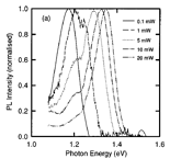 | G Li, C Jagadish, MB Johnston, M Gal
Appl. Phys. Lett., 69:4218-4220 (Dec 1996)
[
pdf ][ SI ][ ref ]
We have optimized growth conditions of metal organic vapor phase epitaxy (MOVPE) in order to grow Si and C delta-doped nipi doping superlattices in GaAs. Trimethylaluminium (TMAl) and silane (SiH4) were used as p-type and n-type doping precursors, respectively. We report that at 630 degrees C, full compensation of free electrons and holes can be obtained in the MOVPE-grown Si and C delta-doped nipi doping superlattices over a very wide range of the sheet carrier densities (10(12)-10(13) cm(-2)) by choosing proper TMAl flow rate and Si delta-doping time or SiH4 flow rate. The experimental results on electrical and optical characterization of Si and C delta-doped nipi doping superlattices in GaAs with 150 Angstrom thick undoped spacer layers are presented. (C) 1996 American Institute of Physics.
Citations: 16 (Scopus) 13 (Web of Science) |
- Effects of anodic oxide induced intermixing on the structural and
optical properties of quantum wire structure grown on nonplanar GaAs
substrate
-
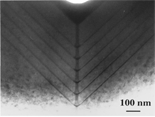 | Y Kim, S Yuan, R Leon, C Jagadish, M Gal, MB Johnston, MR Phillips, MAS Kalceff, J Zou, DJH Cockayne
J. Appl. Phys., 80:5014-5020 (Nov 1996)
[
pdf ][ SI ][ ref ]
Effects of anodic oxide induced intermixing on the structural and optical properties of stacked GaAs quantum wire (QWR) structures grown on a sawtooth-type nonplanar GaAs substrate are investigated. Cross-sectional transmission electron microscope (XTEM) observation, temperature dependent photoluminescence (PL) and cathodoluminescence (CL) imaging were used. Intermixing was achieved by pulsed anodic oxidation of the GaAs cap layer and subsequent rapid thermal annealing, was verified by XTEM analysis. A significant enhancement of QWR PL is observed accompanied by a notable blueshift of the sidewall quantum well (SQWL) PL due to the intermixing. Furthermore, an extended necking region is observed after the intermixing by spatially resolved CL. The temperature dependence of the PL intensities of both SQWL and QWR show maxima at approximately T similar to 110 K indicating the role of the extended necking region in feeding carriers to SQWL and QWR. (C) 1996 American Institute of Physics.
Citations: 19 (Scopus) 21 (Web of Science) |
- Static Electrification by Nonwetting Liquids. Contact Charging and Contact Angles
-
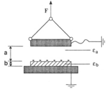 | VV Yaminsky, MB Johnston
Langmuir, 11:4153-4158 (Oct 1995)
[
pdf ][ SI ][ ref ]
A glass slide hydrophobized with dimethyldichlorosilane appears to be electrostatically charged when a nonwetting liquid recedes from its surface. The surface charge has negative polarity. The density of the charge which arises on retraction from water is 10(-4) C/m(2). The half-life of the charge on the surface in air is 0.5 h. The charging effect is observed with different liquids and solutions for which contact angle and surface tension are high. A correlation of the value of the charge with the conductivity and double layer parameters is not pronounced. The electrification leads to a long range attraction between the plate and the liquid and influences the wetting of the substrate.
Citations: 22 (Scopus) 23 (Web of Science) |
|
|
|