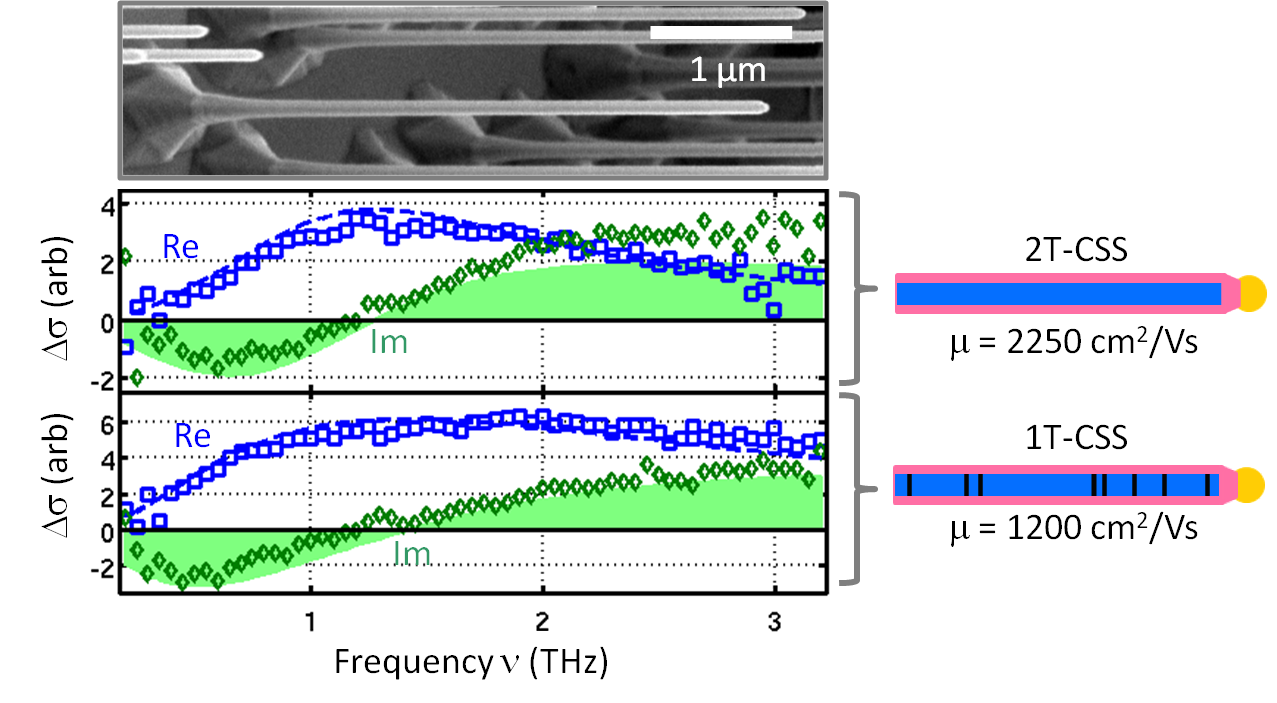
- Resonance-amplified terahertz near-field spectroscopy of a single nanowire
- Norman et al. Nano Lett., 24:15716--15723 (Nov 2024)
[
pdf ][ DOI:10.1021/acs.nanolett.4c04395 ]
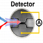
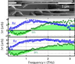
A resonance-amplified terahertz near-field spectroscopy technique is demonstrated that exploits a bowtie antenna to sensitively probe ultrafast conductivity changes in a single InAs nanowire, enabling quantitative extraction of photoexcited carrier dynamics with sensitivity to conductivity variations corresponding to as few as 100 additional charge carriers. |
- Three-dimensional cross-nanowire networks recover full terahertz state
- Peng et al. Science, 368:510--513 (May 2020)
[
pdf ][ DOI:10.1126/science.abb0924 ]
We have developed a new nanowire-based THz sensor that recovers the full state of THz pulses. |
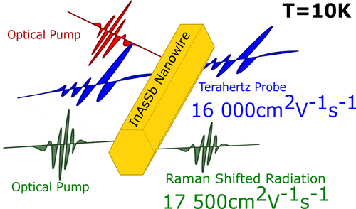
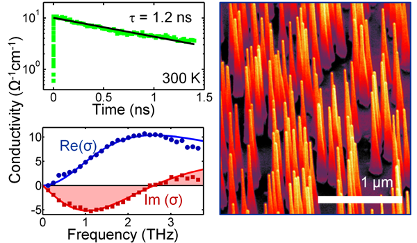
- High electron mobility and insights into temperature-dependent scattering mechanisms in inassb nanowires
- Boland et al. Nano Lett., 18:3703-3710 (Jun 2018)
[
pdf ][ DOI:10.1021/acs.nanolett.8b00842 ]
THz and Raman probes reveal very high electron mobility in InAsSb nanowires, and temperature dependent THz measurement reveal charge-carrier scattering mechanisms |
- The influence of surfaces on the transient terahertz conductivity and electron mobility of {GaAs} nanowires
- Joyce et al. J. Phys. D-Appl. Phys., 50:224001 (Jun 2017)
[
pdf ][ DOI:10.1088/1361-6463/aa6a8f ]
Here we use optical-pump-terahertzprobe spectroscopy to quantify how mobility and lifetime depend on the nanowire surfaces and on carrier density in unpassivated GaAs nanowires. |
- Towards higher electron mobility in modulation doped {GaAs/AlGaAs} core shell nanowires
- Boland et al. Nanoscale, 9:7839-7846 (Jun 2017)
[
pdf ][ DOI:10.1039/c7nr00680b ]
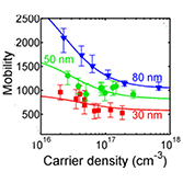
Here we determine donor ionisation energies of Gas/AlGaAs nanowires and study the influence of ionised donors on charge dynamics |
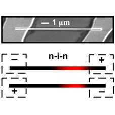
- Single $n^+$-i-$n^+$ {InP} nanowires for highly sensitive terahertz detection
- Peng et al. Nanotechnology, 28:125202 (Mar 2017)
[
pdf ][ DOI:10.1088/1361-6528/aa5d80 ]
|
- A review of the electrical properties of semiconductor nanowires: insights gained from terahertz conductivity spectroscopy
- Joyce et al. Semicond. Sci. Technol., 31:103003 (Oct 2016)
[
pdf ][ DOI:10.1088/0268-1242/31/10/103003 ]
A comprehensive review on how to measure the electrical properties of semiconductor nanowires with THz radiation. |
- Broadband phase-sensitive single {InP} nanowire photoconductive terahertz detectors
- Peng et al. Nano Lett., 16:4925-4931 (Aug 2016)
[
pdf ][ DOI:10.1021/acs.nanolett.6b01528 ]
We present antenna-optimized photoconductive detectors based on single InP nanowires with superior properties of high carrier mobility and low dark current, which exhibit excellent sensitivity and broadband performance. |
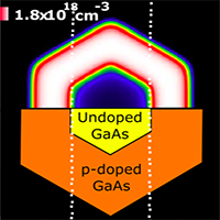
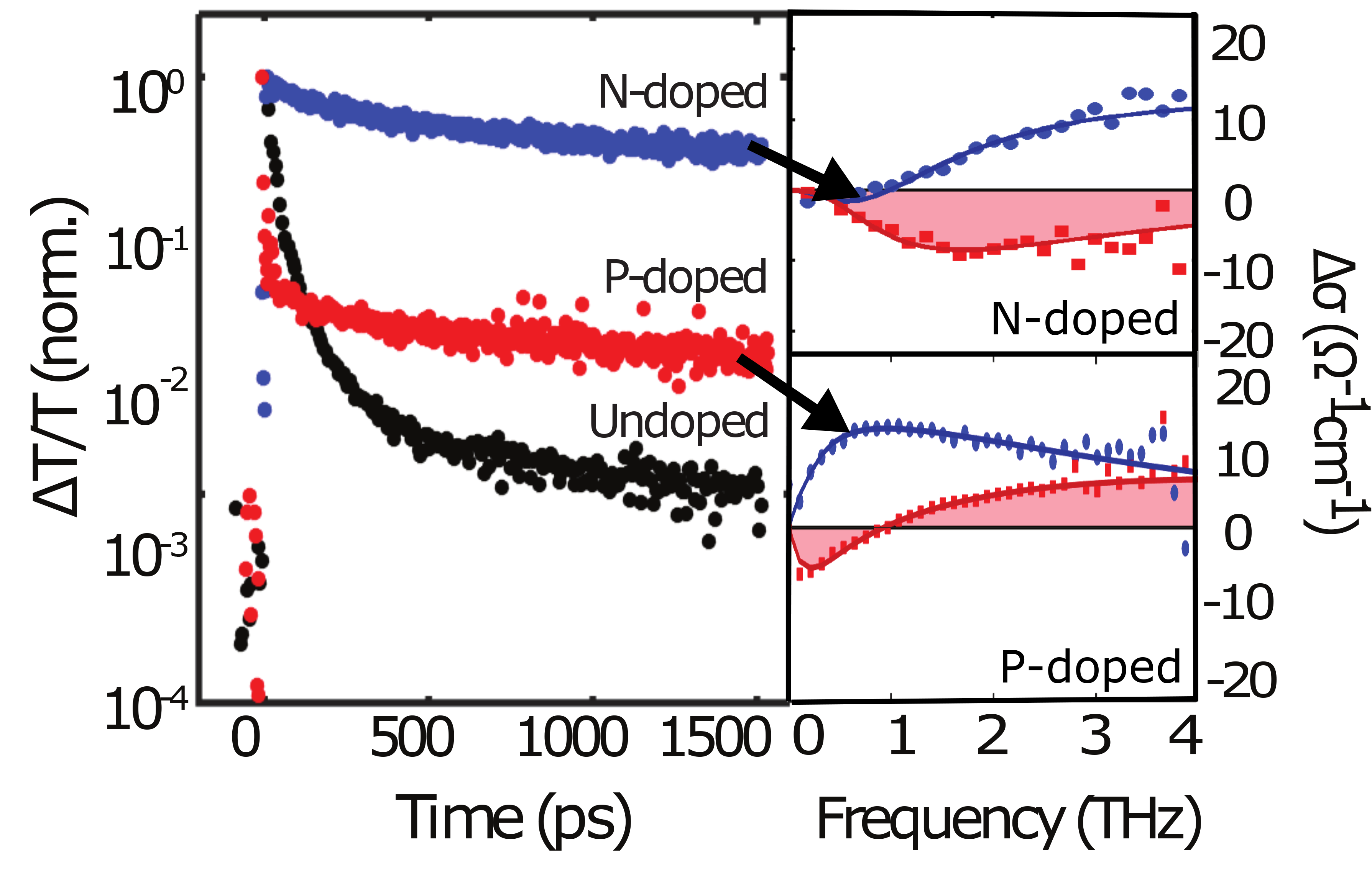
- Increased Photoconductivity Lifetime in GaAs Nanowires by Controlled n-Type and p-Type Doping
- Boland et al. ACS Nano, 10:4219-4227 (Mar 2016)
[
pdf ][ DOI:10.1021/acsnano.5b07579 ]
Terahertz spectroscopy of GaAs nanowires with controlled n-type and p-type shell doping, to show enhanced lifetimes due to reduced surface recombination caused by doping-related band bending. |
- Low Ensemble Disorder in Quantum Well Tube Nanowires
- Davies et al. Nanoscale, 7:20531--20538 (Dec 2015)
[
pdf ][ DOI:10.1039/C5NR06996C ]
This work examines co-axial core-shell nanowires and demonstrates the importance of high quality core growth prior to shell deposition. |
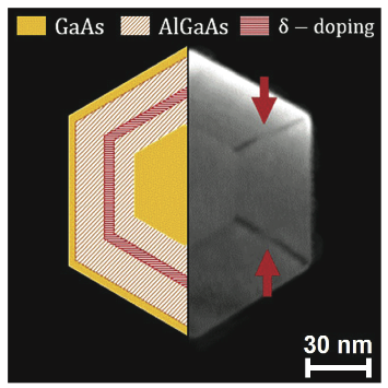
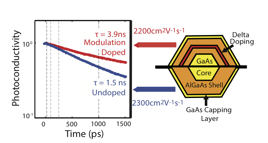
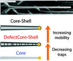
- Modulation Doping of GaAs/AlGaAs Core--Shell Nanowires With Effective Defect Passivation and High Electron Mobility
- Boland et al. Nano Lett., 15:1336-1342 (Jan 2015)
[
pdf ][ DOI:10.1021/nl504566t ]
We demonstrate effective modulation doping in GaAs nanowires. n-doping results in very long photoconductivity and PL lifetimes of 3.9ns and 2.4ns, in these nanowires. |
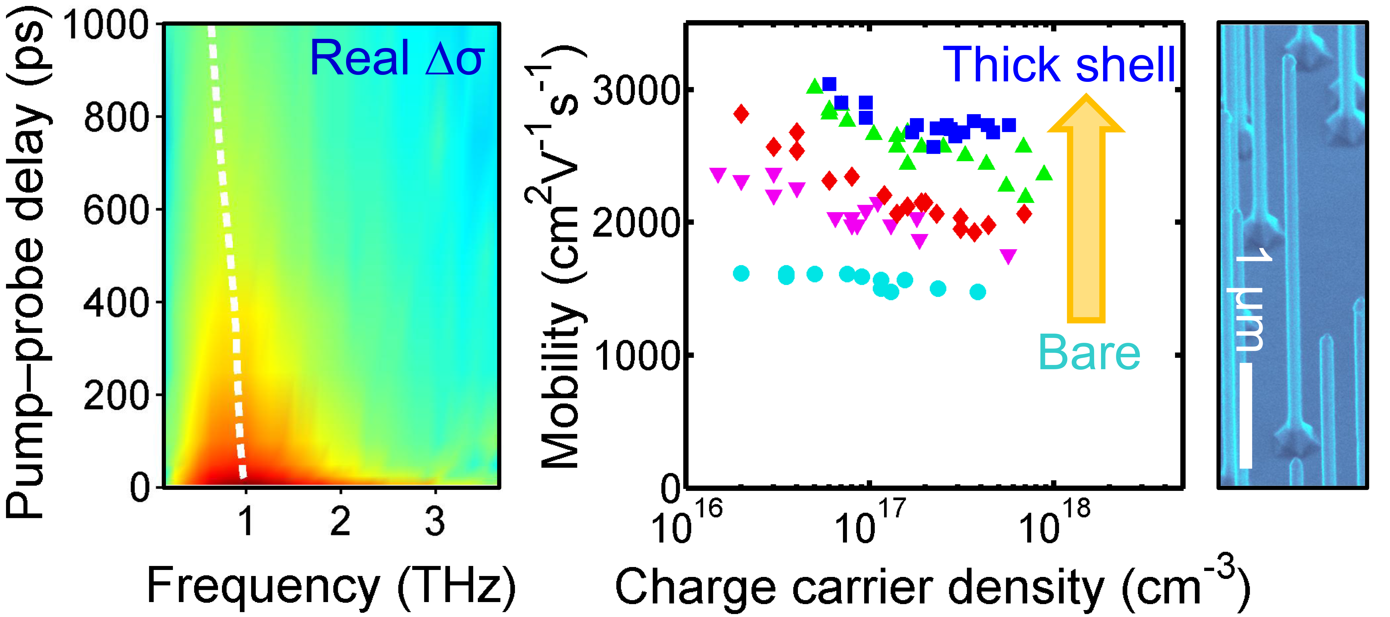
- Electron Mobilities Approaching Bulk Limits in ``Surface-Free'' {GaAs} Nanowires
- Joyce et al. Nano Lett., 14:5989-5994 (Sep 2014)
[
pdf ][ DOI:10.1021/nl503043p ]
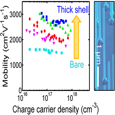
We demonstrate that engineering the GaAs nanowire surface by overcoating with optimized AlGaAs shells is an effective means of obtaining exceptionally high carrier mobilities and lifetimes. |
- Electronic properties of {GaAs}, {InAs} and {InP} nanowires studied by terahertz spectroscopy
- Joyce et al. Nanotechnology, 24:214006 (May 2013)
[
pdf ][ DOI:10.1088/0957-4484/24/21/214006 ]
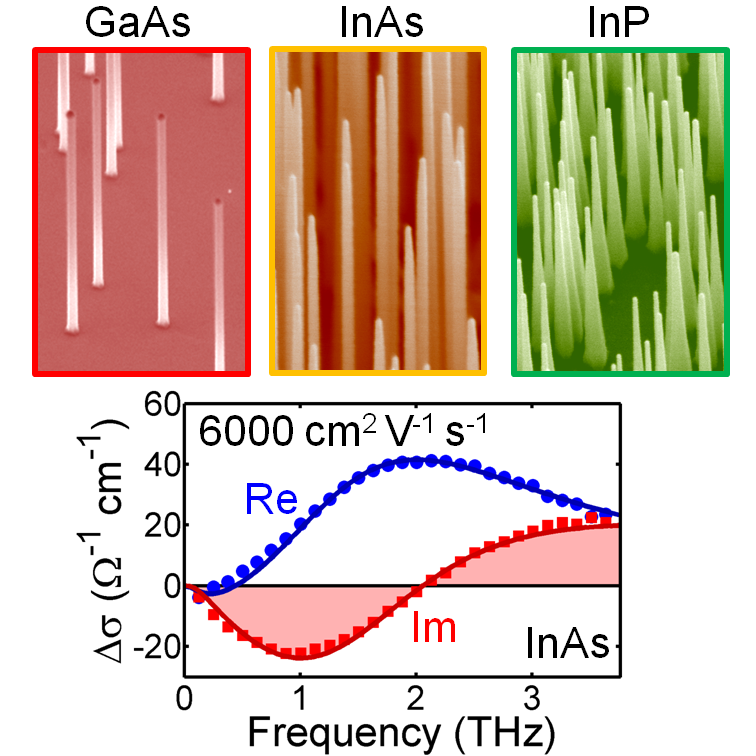
Using terahertz conductivity spectroscopy, we have assessed the ultrafast electronic properties of GaAs, InAs and InP nanowires. InAs nanowires exhibited extremely high electron mobility, highlighting their immediate suitability for high mobility devices. InP nanowires exhibited the longest carrier lifetimes, highlighting their potential for photovoltaics. |
- Ultra-low Surface Recombination Velocity in InP Nanowires Probed by Terahertz Spectroscopy
- Joyce et al. Nano Lett., 12:5325-5330 (Oct 2012)
[
pdf ][ DOI:10.1021/nl3026828 ]
Using terahertz spectroscopy we measured long charge carrier lifetimes and a remarkably low surface recombination velocity in InP nanowires. We found that the carrier mobility is strongly limited by the presence of crystallographic defects, such as zinc-blende/wurtzite polytypism and stacking faults in these InP nanowires. |
- Noncontact Measurement of Charge Carrier Lifetime and Mobility in {GaN} Nanowires
- Parkinson et al. Nano Lett., 12:4600--4604 (Sep 2012)
[
pdf ][ DOI:10.1021/nl301898m ]
We use terahertz spectroscopy to shown that GaN nanowires are electrically superior to bulk GaN. |
- {III}--{V} semiconductor nanowires for optoelectronic device applications
- Joyce et al. Prog. Quantum Electron., 35:23-75 (Mar 2011)
[
pdf ][ DOI:10.1016/j.pquantelec.2011.03.002 ]
III-V nanowires are prime candidates for future quantum electronic devices. This review discusses recent advances in the growth and characterisation of these nanowires, with particular emphasis on terahertz conductivity spectroscopy. |
- Carrier lifetime and mobility enhancement in nearly defect-free core--shell nanowires measured using time-resolved terahertz spectroscopy
- Parkinson et al. Nano Lett., 9:3349-3353 (Sep 2009)
[
pdf ][ DOI:10.1021/nl9016336 ]
We demonstrate that two-temperature growth of the GaAs Nanowires leads to an almost doubling in charge-carrier mobility and a tripling of carrier lifetime. We also show that overcoating the nanowires enhances the charge conductivity. |
- Transient terahertz conductivity of {GaAs} nanowires
- Parkinson et al. Nano Lett., 7:2162-2165 (Jul 2007)
[
pdf ][ DOI:10.1021/nl071162x ]
We observe the dynamic motion of surface plasmons in GaAs nanowires on picosecond timescales using pump-probe THz spectroscopy. The electron mobility is remarkably high, at 1/3 of bulk GaAs at room temperature.
|